Please select your location and preferred language where available.
Technology Topics
Introducing the latest technologies being researched and developed at KIOXIA Corporation and various use cases of flash memories.
-
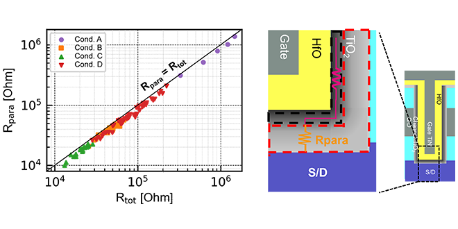
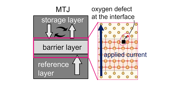
We proposed a guideline for the reduction of parasitic resistance in channel-all-around TiO2 FeFETs based on in-depth electrical analysis. We revealed that the non-accumulated TiO2 channel is the main component for the parasitic resistance and demonstrated its 98% reduction by process optimization.
-
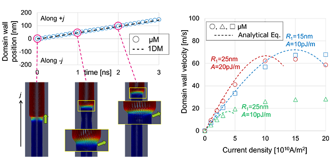
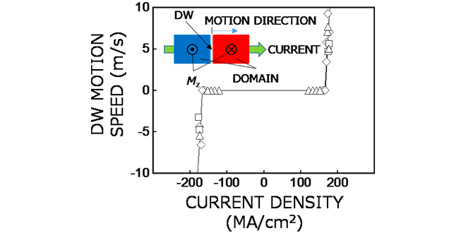
We theoretically investigated the behavior of domain walls (DWs) in nanotubes with perpendicular magnetic anisotropy (PMA). We formulated a model for spin-orbit torque-driven DW motion, enabling rapid quantitative prediction of DW shift characteristics. We presented important insights for device design, showing that DW velocity can be controlled by adjusting the nanotube diameter and magnetic properties.
-
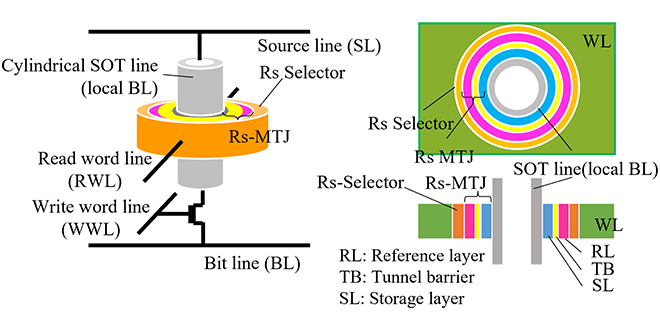
Spin-orbit torque magnetic random access memory (SOT-MRAM) is expected to be a new memory with high-speed operation and low power consumption. Conventional MRAM faced challenges with external magnetic fields disturbance, but as a solution, a ring-shaped magnetic tunnel junction (MTJ) element with a closed magnetic circuit was proposed. The micro-magnetic simulation demonstrated that the storage layer of the Ring-shaped MTJ exhibits a stable coherent magnetization reversal.
-
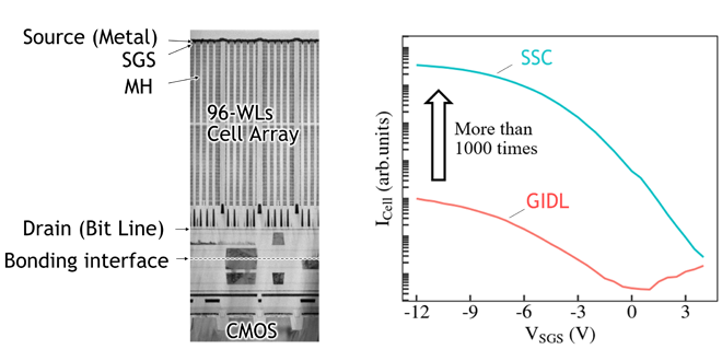
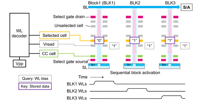
As the number of word lines increases in 3D flash memory, erase speed degradation is expected to become a significant issue. In this work, we propose a novel Schottky source junction that drastically enhances erase operation. The proposed structure was experimentally demonstrated using a prototype cell array. These results were presented at the 2025 IEEE Symposium on VLSI Technology and Circuits.
-
We demonstrated a highly reliable vertical gate-all-around transistor with an oxide-semiconductor channel in a scaled dimension by process and structural optimization. This achievement proves that the oxide-semiconductor transistor technology is promising for future new memory application.
-
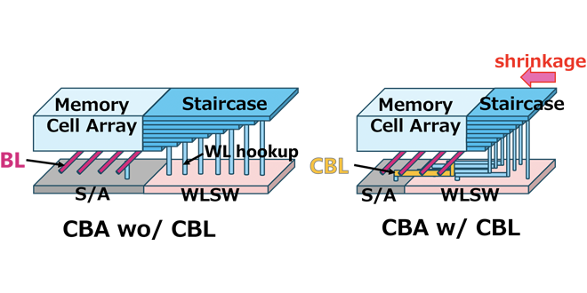
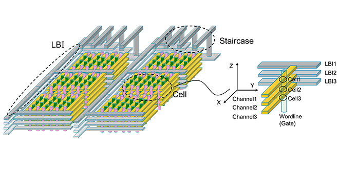
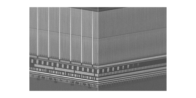
By adopting CBL(Crossed Bit Line) Architecture which is compatible with the CBA(CMOS directly Bonded to Array) technology in BiCS FLASH™ 8th generation, we achieved a 12% reduction in chip size. With the employment of CBL, we improved the sense amplifier operation. Furthermore, the adoption of OPS(On Pitch SGD) leaded to a 15% reduction in memory array area and a 4% reduction in read current.
-
We developed in-memory computing technology using 3D flash memory. This technology is fully compatible with conventional 3D flash memory and it can significantly improve the memory access energy efficiency. This achievement was presented at the IMW 2025.
-
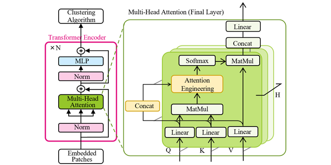
We have developed Inference-Time Attention Engineering (ITAE), which can be applied to AI models, specifically Vision Transformers, for image processing. Our findings confirm that ITAE enhances clustering accuracy across multiple image datasets without the need for additional training on the pre-trained model. We have presented these results at the Asian Conference on Computer Vision 2024, an international conference focused on vision-based AI.
-
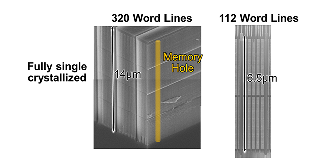
BiCS FLASH™ generation 10 is high memory density 3D flash memory which is well-scaled to 29Gb/mm2 with 332 world-lines stacked and our layout optimization technique, and it achieved the highest bit density and smallest chip in the 1Tb products. We also realized 4.8Gbps data transfer rate and 29% improvement on read energy consumption with new Interface circuit and read operation method.
-
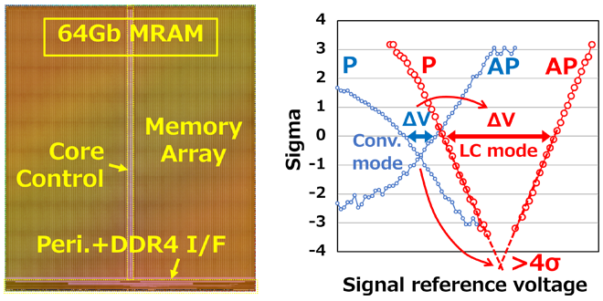
The world’s highest density 64Gbit cross-point MRAM chip with 1Selector-1MTJ cell has been developed. The work presents a novel reading scheme, which enables a high-speed 3ns read pulse and a read margin of over 4-sigma, while addressing read disturbances using the smallest cell size to date.
-
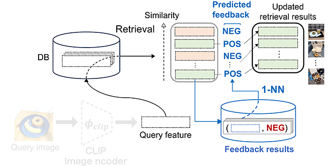
We make foundation-model-based image retrieval able to handle various user’s preferences by leveraging relevance feedback. The proposed approach is empirically effective in various image retrieval scenarios.
-
We fabricated a 64 Gbit cross-point MRAM (Magnetic Random Access Memory) with the world’s smallest cell area of 0.001681 μm2 and demonstrated reliable memory cell operation. This achievement paves the way for MRAM applications in SCM (Storage-Class Memory).
-
We proposed the new architecture, Horizontal channel flash, which enables further cost reduction for future 3D flash memory. We also examined its cell characteristics and confirmed 10k cycle program/erase operations on a test device. This achievement was presented at the IEDM 2024.
-
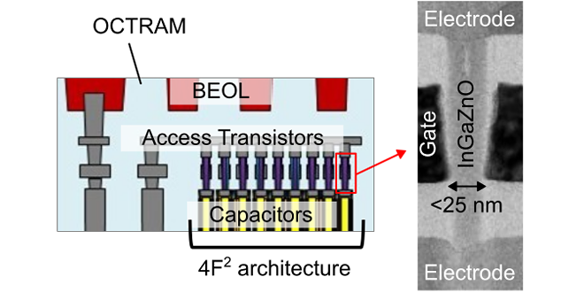
Kioxia, in collaboration with Nanya, developed Oxide-semiconductor Channel Transistor DRAM (OCTRAM) technology. The ultra-low leakage properties of InGaZnO transistors enabled long data retention over 100 sec, providing significant advantages in power saving compared to conventional DRAM.
-
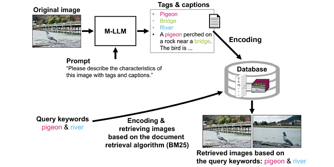
We have developed an image retrieval system that utilizes a multi-modal large language model and a document retrieval algorithm. We have confirmed the performance improvement in the keyword-based retrieval scenario.
-
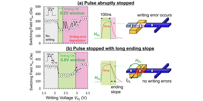
We are developing magnetic domain wall memory as one of the candidates for a new file memory. We have proposed and demonstrated a novel stable writing scheme where writing is performed by the current-induced magnetic field. By gradually stopping the write current pulse, the device is cooled while applying current magnetic field, achieving the stable writing with low error rate. These results were presented in SSDM 2024.
-
It is well known that electrical resistivity in poly-crystalline metallic interconnects increases with downsizing their critical dimension. This is called as size effect on electrical resistivity. Additionally, an anisotropic property manifests itself in the size effect by single crystallization of metallic interconnects. We have successfully developed a numerical simulation technique to predict the anisotropic size effect on electrical resistivity in the single-crystalline metallic interconnects. This achievement was presented at the SSDM 2024.
-
Metal-induced Lateral Crystallization (MILC) is a crucial technology for the high-stacking 3D flash memory. In this study, MILC mechanism was revealed at the atomic scale by using first-principles calculations. This achievement was presented at the international conference SISPAD 2024.
-
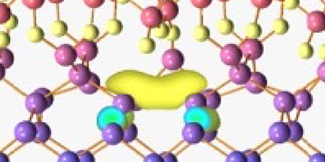
Rapid advances in Artificial Intelligence and Machine Learning are increasing the demand for non-volatile emerging memories with high speed operation. We have demonstrated, for the first time, memory operation of Channel-All-Around FeFET, and realized high ΔIon>2μA and stable endurance (>106cycle) in the smallest footprint ever (707nm2).
-
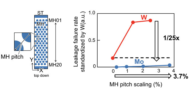
A state-of-the-art fluorine-free word line (WL) molybdenum (Mo) process has been established for future 3D flash memory. Application of Mo to WLs can accelerate scaling of cells in both the vertical and horizontal directions with lower RC delay and lower leakage failure rates compared to traditional tungsten. These results were presented at VLSI 2024.
-
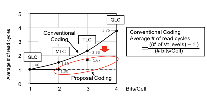
As the number of multi-level increases from MLC, TLC and QLC, while the memory density can be increased, the number of reads increases and random access deteriorates. We reported on a new multi-level coding method that reduces the number of reads and enables high-speed random access while maintaining a high memory density by sharing data among multiple memory cells.
-
We have investigated the stress-time dependent degradation of magnetic tunnel junction (MTJ) in high-density spin-transfer torque magnetic random access memory (STT-MRAM). We have proposed mechanism and suppression methods of the degradation using the density functional theory calculation and time-evolution model. Our findings provide valuable insights into the reliability in high-density STT-MRAM. This achievement was presented at the IRPS 2024.
-
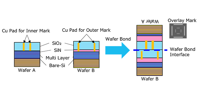
We demonstrated high-precision bonding overlay control techniques using a newly developed overlay measurement tool that uses infrared (IR) light. The accuracy of the IR-light overlay measurement was verified by using a conventional visible-light tool after silicon grind. The results show an excellent correlation between the bonding overlay and overlay after Si grind.
-
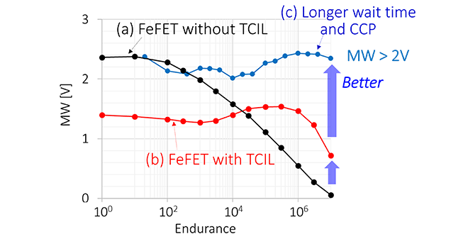
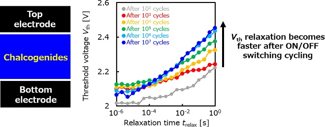
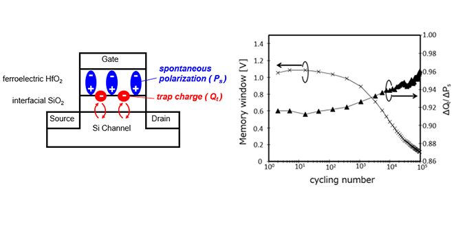
The limited endurance is one of the major challenges in Si channel FeFET, which has attracted much attention as candidates for next-generation memory. By combining trap-controlled interfacial layer (TCIL) and the charge-control operation sequence, MW of >2 V in FeFET has been achieved even after 107 cycles.
-
BiCS FLASH™ generation 8 is our latest high performance and high memory density 3D flash memory. Data are transferred to outside with 3.2Gbps speed, while data are read and programmed inside with 40μs time and 205MB/s throughput, respectively. The memory density of the 1Tb TLC product is well-scaled to 18.3Gb/mm2. We here introduce the two new technologies applied in order to enhance performance and the memory density: CBA (CMOS directly Bonded to Array) and OPS (On Pitch SGD).
-
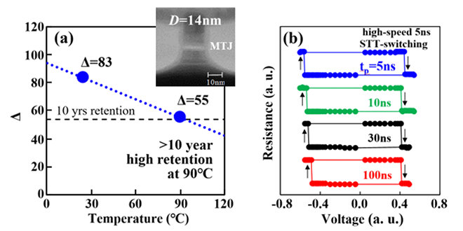
We have demonstrated a novel 14nm magnetic tunnel junction(MTJ) for achieving high-retention and high-speed writing simultaneously in 1Z (15-14) nm Spin-Transfer-Torque(STT) MRAM. Our MTJ, called as AccelHR-MTJ(Accelerated STT-Switching and High-Retention MTJ), can show excellent performances such as high-retention of >10 years at 90℃ and high-speed writing down to 5ns. This achievement was presented at the IEDM 2023.
-
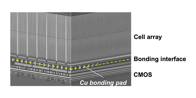
CMOS directly bonded to array(CBA) technology with Cu direct bonding process has been developed and applied to BiCS FLASH™ generation 8 for performance improvement and cost reduction of 3D flash memory.
-
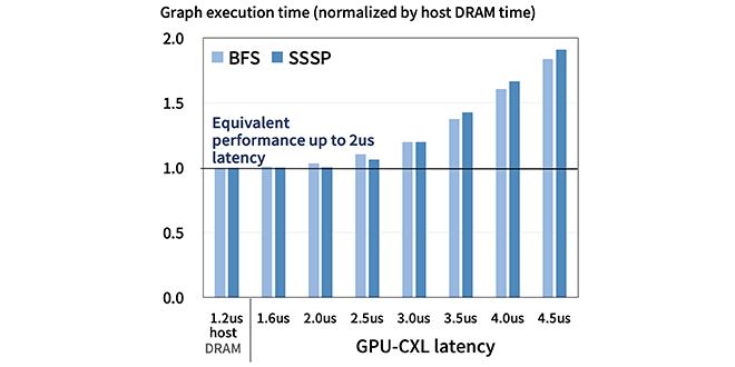
We are evaluating Compute Express Link™(CXL) memory as external memory for GPUs. We have demonstrated GPU graph processing speeds close to using the host DRAM when the CXL memory latency is under a few microseconds. This indicates the possibility of replacing DRAM with low-latency flash to achieve a cost-effective system.
-
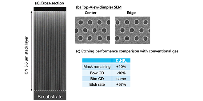
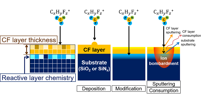
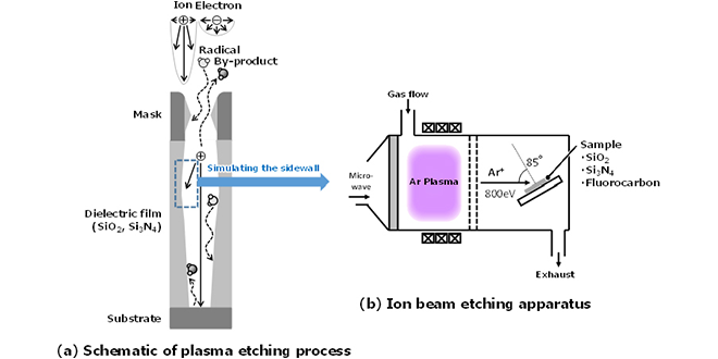
Memory hole etching of 3D flash memory devices requires high throughput and a well-controlled hole profile. Here, we summarize our new etching technology using a novel, environmentally friendly C3HF5 gas. These results were presented at the international DPS2023 conference.
-
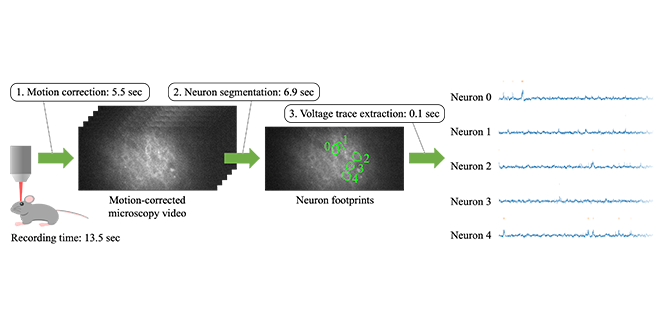
We are developing high-speed microscopy image processing methods leveraging SSDs. One of them is a method able to extract neural voltage from microscopy video in real time, and we presented it at the International Conference on Bioinformatics and Biomedicine (BIBM) 2023.
-
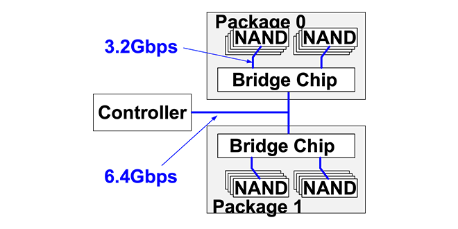
We have developed a Bridge Chip provides twice the speed of existing NAND interfaces even with multiple packages on each PCB channel. A NAND Flash Memory Multi-Chip Package incorporating both eight 1-Tb NAND dies and developed Bridge Chip can operate at 6.4Gbps/pin.
-
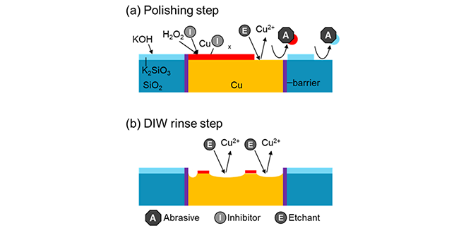
We investigated the dishing reduction of Cu bonding pads in the CMOS directly Bonded to Array(CBA) process, a new architecture for 3D flash memory. We found that the suppression of chemical etching during CMP can reduce dishing and improve yield. These results were presented at the international conference ICPT 2023.
-
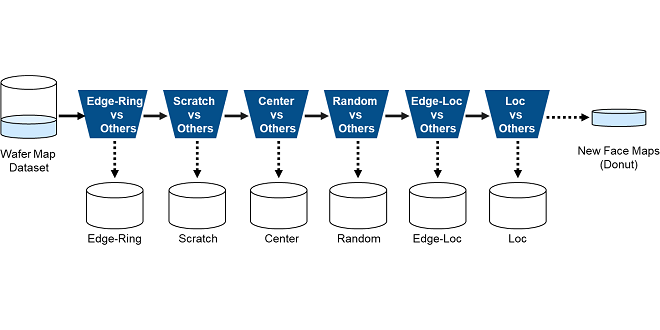
We have studied with Mie University to improve the accuracy of wafer map(data representation showing which chips on a wafer are defective) classification, which is used to investigate the causes of defects in the semiconductor manufacturing process. The method devised in this joint research was presented at the AEC/APC Symposium Asia 2023.
-
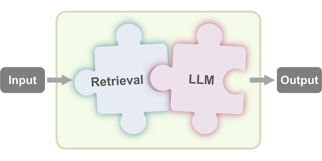
We developed the accessible frameworks for developing and evaluating retrieval-augmented large language models.
-
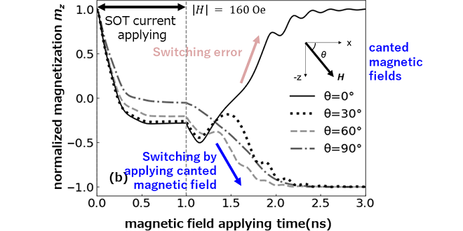
Spin orbit torque(SOT) driven magnetization switching has recently attracted attention towards next generation magnetic memory. In this report, we newly introduced a canted bias magnetic field and clarified that it makes the SOT driven perpendicular magnetization switching faster and more stable. This was presented at International Conference on Solid State Devices and Materials in 2023(SSDM2023).
-
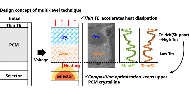
We demonstrated a multi-level phase change memory (PCM)/Selector cell which can be programmed without iterative verify operation. Optimal thermal and composition design enabled to form distinct middle resistance state, in which crystalline and amorphous co-exist at designed positions. Multi-level programming was achieved by one single pulse, and it was stable over 107 cycles, making it promising for future cost-effective, large-capacity, and high-speed cross-point memory.
-
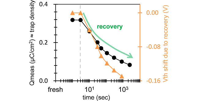
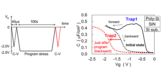
HfO2-based Ferroelectric Field-Effect Transistor (FeFET) is a promising candidate for next-generation memory. This study clarified that program/erase cycling generated new trap sites in interfacial SiO2 layer disappears with time. This recovery phenomenon has a non-negligible impact on the threshold voltage behavior during retention process. These results were presented at the international conference SSDM 2023.
-
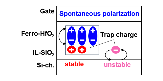
Imprint* is one of the critical reliability challenges in HfO2-FeFET, which has attracted attention as candidates for emerging high-speed memory devices. We have clarified the relationship between spontaneous polarization, trap charge, and imprint by charge component analysis. This result was presented at the international conference SSDM2023.
* Phenomenon in which the voltage required for polarization reversal(coercive voltage Vc) in a ferroelectric film shifts while the polarization state is maintained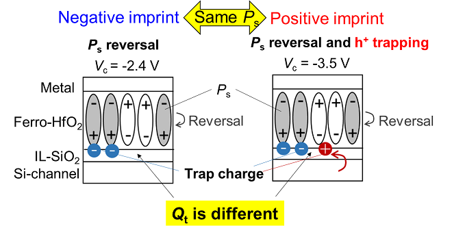
-
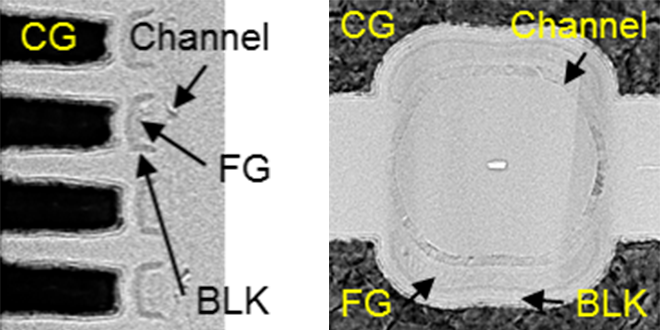
The crystallization technology for Si channel, using metal-assisted materials, has been developed for 3D (three-dimensional) flash memory. It has successfully achieved cell array operation for the first time. This approach can reduce the density of grain boundaries in the Si channel, leading to reduction in trap density in Si channel compared to conventional polycrystalline Si channel. As a result, this technology can realize lower channel resistance, smaller RTN (random telegraphic noise) and narrower threshold voltage distribution in QLC (quadruple level cell) operation.
-
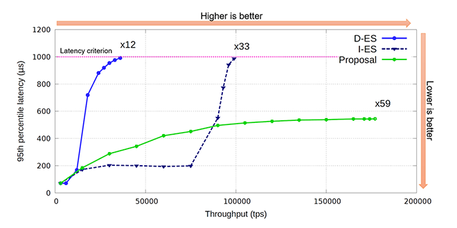
The erase operation of flash memory is one of the causes of performance degradation in SSDs. We have developed an efficient erase technology for low-latency flash memory-based SSDs and achieved a significant performance improvement in a database application evaluation.
-
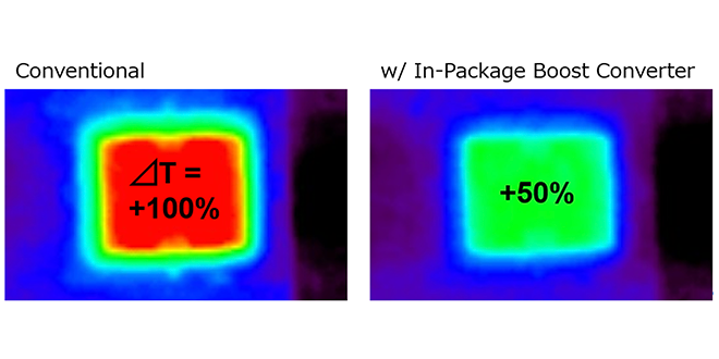
We have developed a package that incorporates 3D flash memory and a boost circuit using a DC-DC converter. This technology can drastically reduce power consumption and operating temperatures, enabling the thermal throttling-less SSD even if the number of Word-line stacked layers reaches 1,000 in the future. This achievement was presented at the International Memory Workshop 2023.
-
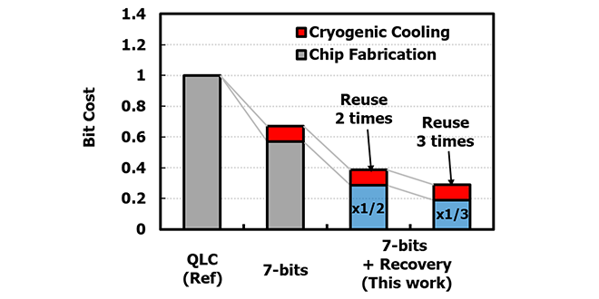
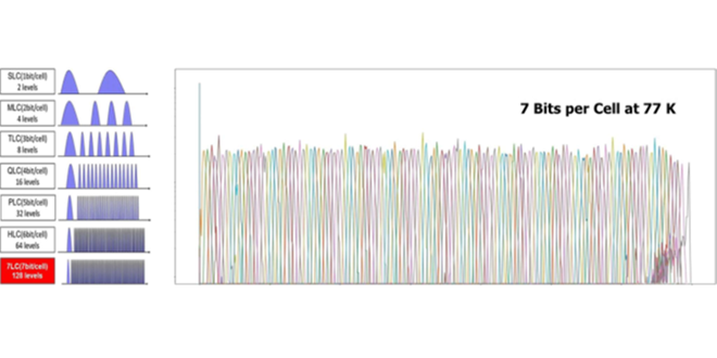
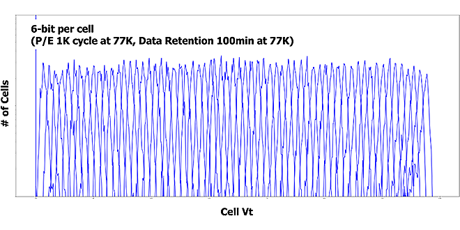
We developed a recovery annealing technology applicable to 7-bit per cell flash memory operating at cryogenic temperatures. The technology can contribute to the realization of a sustainable society through future bit cost scaling and extended chip life.
-
We have successfully demonstrated the preparation of ferromagnetic Co thin layers showing the current-induced domain wall motion (CIDWM), by using atomic layer deposition technique which is widely utilized in the three-dimensional LSI technologies. CIDWM is the key physical phenomenon for race-track memory[1]. This result was presented in the international conference, IEEE INTERMAG 2023[2].
-
We developed new analysis method which can evaluate trap characteristics in short time domain. And we clarified whole picture of hole trapping in SiN film which is essential to improve charge trap memory devices. These results were presented at the international conference IRPS 2023.
-
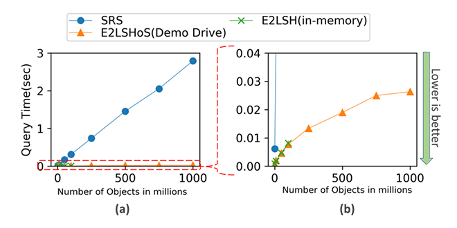
Locality Sensitive Hashing (LSH) is an approximate nearest neighbor search method widely used for big data search and retrieval. By effectively introducing flash memory and developing a new algorithm, we have improved LSH and achieved significant performance improvement by reducing the overhead of computation and external storage access without increasing the main memory.
-
HfO2-based FeFET is a promising candidate for next-generation memory. The coupling between polarization reversal and charge trapping was revealed in this study. We demonstrated a novel operation scheme that strongly suppresses unintended programing of FeFET during memory array operation. These results were presented at the international conference IRPS 2023.
-
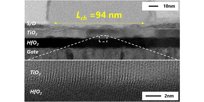
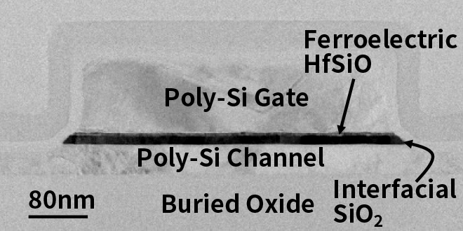
Ferroelectric MOS transistors using HfO2 as the dielectric and Si as the current path have been widely researched and developed for memory applications including AI applications. Kioxia has fabricated a prototype ferroelectric Field Effect Transistor (FET) using TiO2 as the current path and demonstrated high-speed, low-voltage operation and high cycle endurance. This achievement received the Best Contributed Paper Award at the international conference EDTM2023.
-
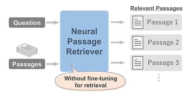
We developed a zero-shot passage retrieval method which employs a pre-trained neural language model without fine-tuning for retrieval. The proposed method achieves almost comparable performance to state-of-the-art passage retriever when a named entity in a question is a dominant clue for retrieval, where conventional neural retrievers have struggled to perform.
-
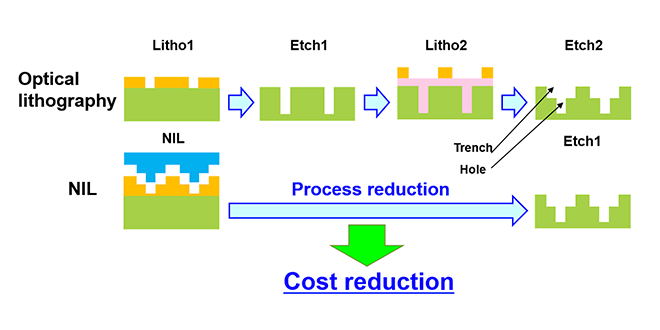
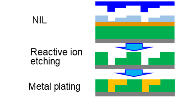
3D patterning is a unique feature of Nanoimprint lithography (NIL). We have studied fabrication of 3D dual-damascene structure using NIL. By optimizing the resist material, template structure, NIL conditions, and etching conditions, respectively, we succeeded in fabricating 3D dual-damascene structure with L/S=4X/4Xnm.
-
Selector devices are key components for next-generation high-density memory cell arrays. In this work, the reliability of selector devices has been studied in collaboration with imec, the world-leading R&D center in electronics technologies. The mechanism of the cycling-dependent threshold voltage instability has been clarified by combining electrical characterization and modeling techniques. These results were presented at the international conference IEDM2022.
-
As the demand for larger memory capacities has rapidly increased, a high etch rate for a high aspect ratio structure is significantly required for high productivity. We have modeled ion-induce surface reactions and developed a simulation technique for predicting the optimal ion species for the etching process of the memory hole because ion species play a dominant role in high aspect ratio etching.
-
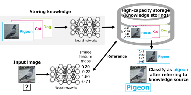
We developed a Memory-Centric AI-based image classification system that utilizes high-capacity storage to enable knowledge expansion while avoiding catastrophic forgetting. It improves explainability of AI by retaining the reference images used for classification.
-
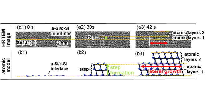
In 3D LSI, transistors are formed on polysilicon. The formation of defect-free polysilicon is important for high performance transistors. To establish the formation process, we improved the conventional electron microscope technology and observed the growth process of crystal grains on an atomic scale in real time.
-
November 30, 2022 Frontier Technology R&D Institute (System Technology)
We developed the technique for avoiding false-lock points induced by PAM4 signaling by switching the comparator mode between NRZ mode and PAM4 mode according to the state of the CDR operation, and confirmed the effectiveness of proposed technique.
-
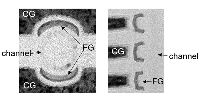
Large program/erase window, tight Vth distributions and superior data retention characteristics, which were essential to achieve multiple bits per cell, realized by optimizing read operation and FG structures in split-gate cells.
-
We investigated the adhesion mechanism between the mold resin and sputtered copper in electromagnetic wave shield packages. We found that the amount of silica filler exposed by etching the mold resin affects the adhesion with copper.
-
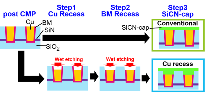
Highly reliable copper interconnect technology is required for the high-voltage circuits of 3D flash memory. We have developed Cu recess interconnect structure and demonstrated that this structure can improve Cu line-to-line reliability.
-
We successfully demonstrated the world’s first 7-bit per cell by combining 77K cryogenic operation with silicon process technology that can improve memory cell characteristics.
-
Two design constraints are introduced to improve process margin of Ultraviolet nanoimprint lithography. One is for NIL alignment mark design rule and the other is for pattern coverage rule with wafer topography.
-
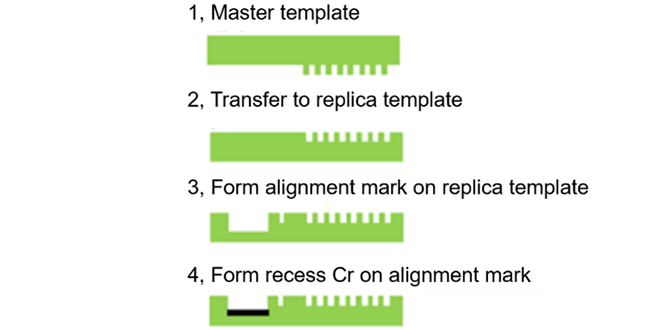
The accuracy of alignment with the underlying layer in UV nanoimprint lithography has been improved by using a method of making separate alignment marks. This enables the practical realization of low-cost patterning with a half-pitch of 14 nm in a single patterning step, which is impossible by optical lithography.
-
Understanding process mechanisms is critical for the development of next-generation BiCS FLASH™. We describe an example using memory hole etching, which is key to designing the memory cell.
-
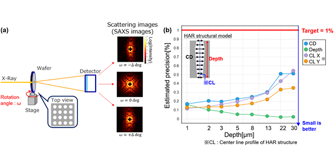
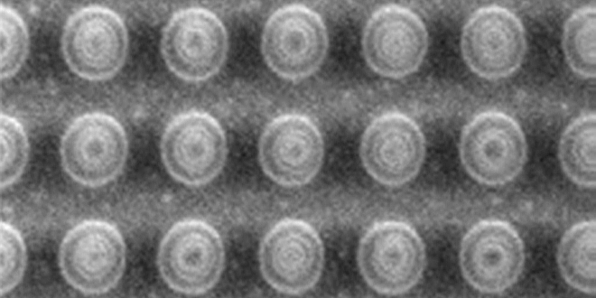
In 3D memory manufacturing, extremely small diameter and extremely deep holes (high aspect ratio) are processed. For this control, a nondestructive and highly accurate measurement method is required. We analyzed the measurement capability of T-SAXS (transmission small angle X-ray scattering) by simulation. We confirmed that T-SAXS can measure structures of 0.1um diameter and 30um depth with <1% accuracy. This achievement is important for realizing future 3D memory.
-
HfO2-FeFETs is a strong candidate for next-generation memory. In HfO2-FeFETs memory the difference between "0" and "1" decreases after repeated write and erase operations. This cycle degradation, which remained largely unknown, has been clarified by high-speed charge center analysis. This achievement is expected to advance the practical application of HfO2-FeFET memory. These results were presented at the international conference IEDM2021.
-
Digitalization of defect data from the device manufacturing processes and design data has dramatically improved the accuracy of electrical test pass/fail prediction.
This technology has contributed to speeding up the device development and improving productivity.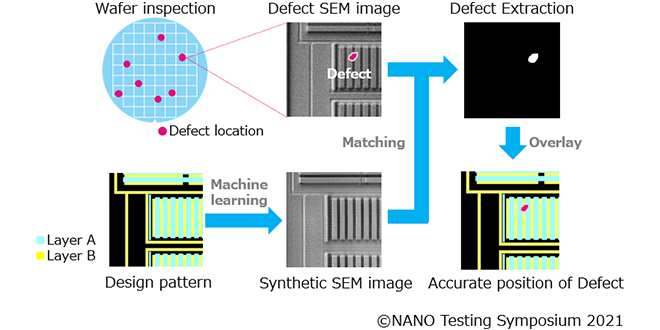
-
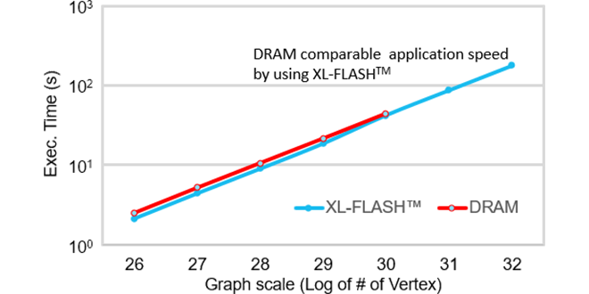
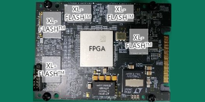
We introduced high-speed flash memory (XL-FLASH™) and developed a new access method for it, achieving the equivalent speed as keeping all graph data in DRAM. This enables high-speed processing for very large-scale graph with flash memory at lower cost than DRAM.
-
With the growth of the quantum computing and high performance computing, there are increasing demands for the computer systems and electrical components that can operate at relatively low temperature. It has been reported that the characteristics of several types of semiconductor devices can be improved by cryogenic temperature. This report is the first to introduce a cryogenic operation and characteristics of 3D Flash memory at 77 K immerged in the liquid nitrogen.
-
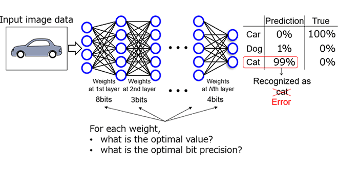
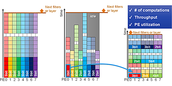
We have developed not only a filter-wise quantization algorithm which optimizes the number of weight bits for each one of tens or thousands of filters on every layer but also the dedicated accelerator. With these algorithm and hardware architecture, the inference time can be reduced while maintaining recognition accuracy.
-
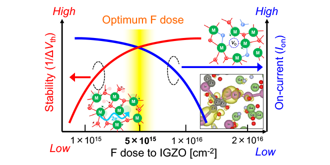
OS-FET with both high thermal stability and high on-current can be realized by optimizing F amount in IGZO:F. These results are fundamental technologies to realize new memory devices with large amounts of storage, low latency, and ultralow-power consumption, which cannot be achieved by silicon-based FETs.
-
Recently, ferroelectric memories using ferroelectric-HfO2 film have attracted much attention towards low-power and high-density in-memory computing for AI (artificial intelligence).
-
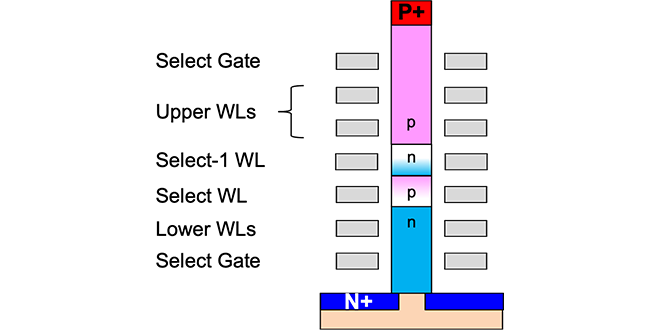
BiCS FLASH™ can increase its memory density and reduce the product cost by increasing the number of word line (WL) layers. The thyristor structure is one of the promising candidates to obtain a large read current even the number of stacked layers is increased.
-
We demonstrate capability of replacing DRAM for a key-value store database using XL-FLASH™, which has lower bit cost and larger capacity than DRAM. In order to evaluate the possibility of DRAM replacement using XL-FLASH™, we have developed XL-FLASH™ demo drive, and demonstrated the evaluation result that the database using DRAM and the database using XL-FLASH™ have equivalent performance in read access-dominated situation.
-
A challenge of OS-transistor development is improvement of its thermal stability. By using InGaZnO (IGZO) which is a conventional OS, the OS transistor does not work properly by thermal processes required in manufacturing process of the memory device.
In order to overcome this issue, we have newly proposed InAlZnO (IAZO) as an OS material with high thermal stability.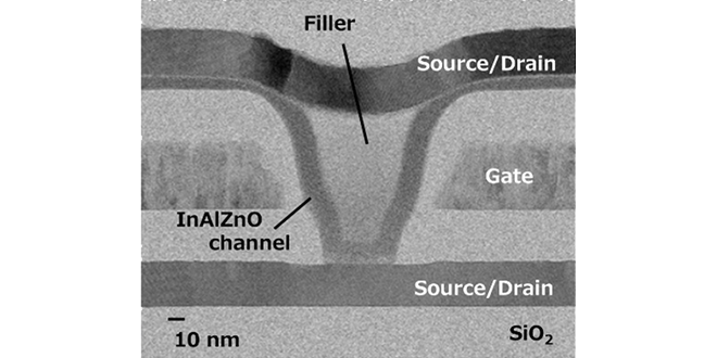
-
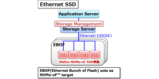
Usually networked storage is implemented on storage servers with multiple SSDs. However, now it becomes true that storage servers cannot fully utilize the high-speed performance and low latency of NVMe SSDs due to the bottleneck of computing power and limited network bandwidth. To solve this problem, Kioxia is developing SSD that connects directly to the network and enables high-speed, low-latency access (Ethernet SSD).
-
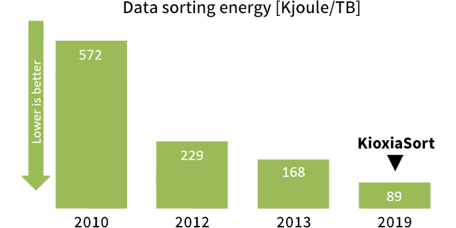
In sort benchmark contest founded by Dr. Jim Gray who was a winner of ACM A.M. Turing Award, there is a category called JouleSort to compete energy consumption in data sorting. Our sorting algorithm KioxiaSort was awarded a JouleSort world record on November 27 in 2019.
-
In order to cope with shrinking of semiconductor device pattern dimension below 30nm half pitch and increasing fabrication cost, we are developing low cost Nanoimprint Lithography (NIL.)
-
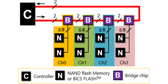
In order to achieve a large-capacity storage using NAND Flash memory and BiCS FLASH™ (hereinafter, referred to as NAND), many NAND packages have to be connected to a controller. We have proposed a daisy-chain configuration using bridge chips, to achieve high-speed operation and large capacity with fewer signal lines.
-
By applying MILC(Metal-induced Lateral Crystallization) technology to Si film in the vertical memory holes, we successfully fabricated the formation of monocrystalline Si from amorphous Si via nickel silicide.
The 3D flash memory cell devices equipped with this technology demonstrated superior electrical characteristics and reduced variation compared to conventional devices using poly-Si as the channel.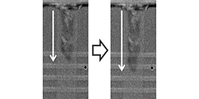
-
Three-dimensional (3D) semicircular split-gate flash memory cells have been successfully developed for the first time.
-
The challenge for achieving terabit-scale cross-point memory is to reduce operation current of a memory cell.
As a solution, we focused on a new non-volatile memory; Ag ionic memory.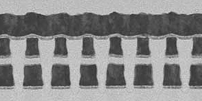
-
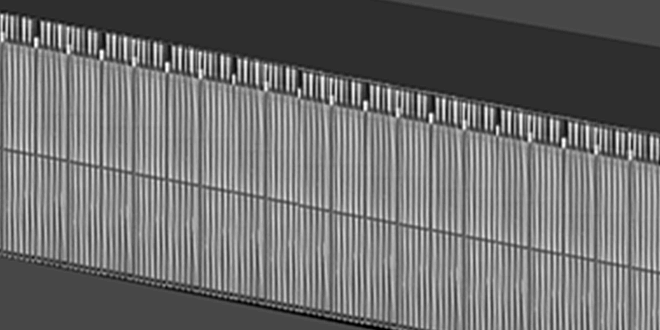
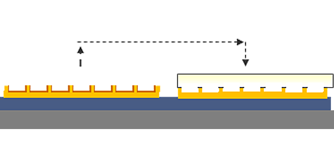
BiCS FLASH™ 3D flash memories, electrode and dielectric layers are alternately stacked all at once, and then holes are punched through all the layers at once, to reduce the number of manufacturing processes. For these manufacturing processes, plasma etching (RIE: Reactive Ion Etching) technology is crucial in order to form deep memory holes with a uniform diameter.
-
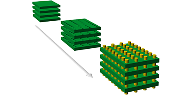
To meet the demand for ever-smaller, higher-capacity storage devices, it is essential to increase the storage density of flash memories. For two-dimensional (2D) NAND flash memories, we have employed nanofabrication and other technologies to develop a 15-nm memory cell, realizing such flash memories. However, geometry scaling is approaching the physical limit. BiCS FLASH™ overcomes the density limit through multilayer cell array stacking.
-
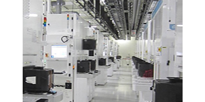
To maintain high quality in our flash memory production, more than two billion data items are collected every day in real time from manufacturing equipments and transport systems. Complicated factory analyses are performed using such an enormous amount of data.
-
We have developed an AI accelerator for deep learning and presented it at an International conference on semiconductor circuits, A-SSCC 2018.
-
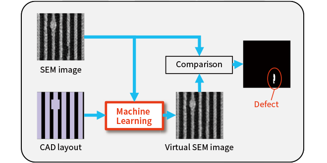
State-of-the-art semiconductor manufacturing requires highly accurate defect inspection even if the defects are very small. We are developing a new inspection technique utilizing not only conventional image processing but also machine learning.
-
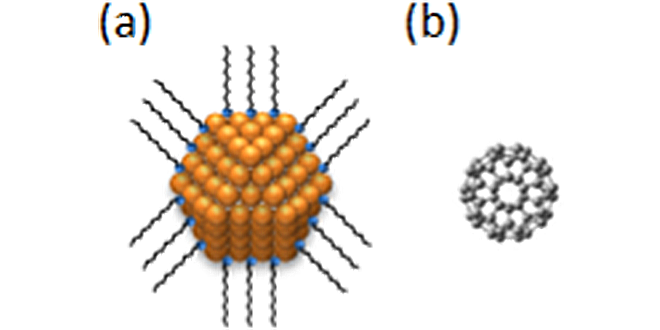
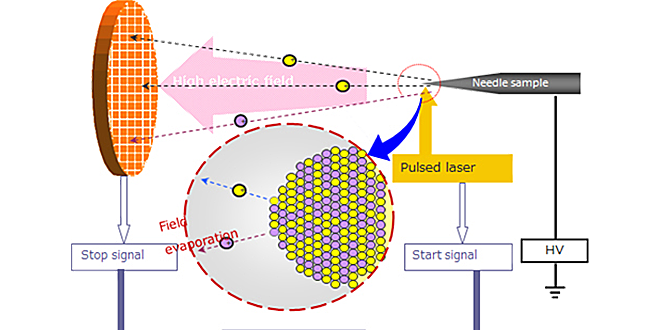
We have established a brand-new evaluation method for nanomaterials by applying the state-of-the-art semiconductor fabrication process.
-
HMB technology utilizes part of the host memory (DRAM) as if it were its own, and achieves equivalent performance to an SSD with DRAM. As cooperation between the host driver and SSD is necessary, we developed HMB protocols for booting and connection, and have them incorporate PCIe® SSD interface standard, NVMe™ 1.2* with major CPU/OS vendors.
* An interface specification developed for SSDs
NVMe is a trademark of NVMe Express, Inc. PCIe is registered trademark of PCI-SIG.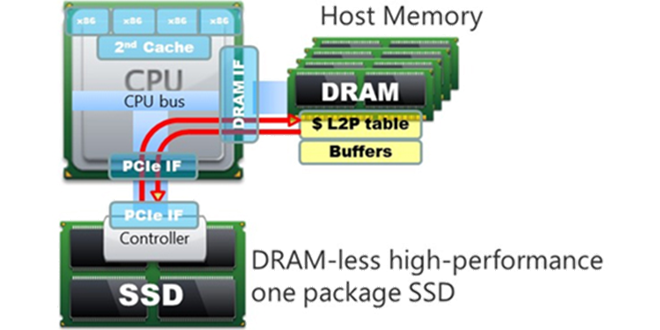
-
As many 3D memory nanostructures consist of intricately stacked thin films, it is very important to accurately understand the nanostructures of individual films, the interfaces between them, and the elemental composition distribution in order to realize high-performance and high-reliability devices. New analytical techniques need to analyze nanometer-level 3D structures, and we are driving various advanced analysis methods to achieve this task.
-
In order to overcome the lithography process cost increase, we are developing nanoimprint lithography that can miniaturize devices at lower cost.
-
Memory devices that require new materials and complex 3D structures.
-
We propose new memory cell technologies to realize even higher bit density file memories, as well as various high-speed nonvolatile memories.
R&D Organization
We aim to pursue continuous technological exploration and its social implementation to achieve an affluent and sustainable digitalized society through innovative memory technologies.

Conducts R&D on BiCS FLASH™, a type of 3D flash memory that KIOXIA was the first to develop in the world, while serving as a bridge between R&D and volume production.

KIOXIA memory and storage solutions enable the success of emerging applications and allow existing technologies to reach their expected potential.

A technical glossary that covers terms related to KIOXIA products and technologies, such as memory and SSDs. We explain that it can be used by engineers and researchers to the general public.

KIOXIA has established industry-leading R&D frameworks with “memory” technology. We use our various locations to conduct technological innovation while promoting open innovation.