Please select your location and preferred language where available.
Technology Development History
Introducing KIOXIA’s achievements in supporting the evolution of electric devices, such as the invention of NAND flash memory in 1987, and advancement of information society on a global scale, seen through the lens of the history of flash memory and SSD development.
*The information on this page is current as of the date of the announcement.
1980s - 1990s
NAND Flash Memory at Dawn
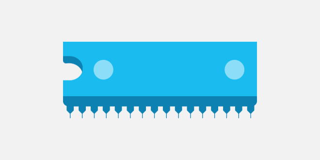
KIOXIA invented the world’s first NAND flash memory in 1987.
NAND flash memory is a storage device that enables large amounts of data to be stored, and it is now an essential part of familiar electronic devices such as smartphones, and data centers.
At the time of commercialization, the mainstream memory capacity was still 4 to 16Mbit (about 1 or 2 songs of music and 1 or 2 photos when converted to the current photo and music data capacity.) From that time, KIOXIA proceeded with development aimed at increasing the capacity with the idea that “flash memory will eventually replace hard disk drives”, and produced breakthrough technology one after another. In 1998, we commercialized 256Mbit NAND flash memory. (256Mbit: about 1 - 2 music CDs / about 16 - 32 photos)
At the time, SSD hadn’t been named “SSD” yet and were called “silicon disk” or “flash drive.”
Advantage of these drives was excellent vibration and shock resistance achieved by not consisting of moving parts such as motors and pickups. For this advantage, they were used in some industrial equipment, but only in a small proportion because drives with NAND flash memory were very expensive compared to HDDs.
|
1984 |
|
|---|---|
|
1987 |
|
|
1991 |
|
|
1992 |
|
|
1995 |
|
|
1997 |
|
|
1998 |
|
Column: Changing Lifestyle with Flash Memory
Digital cameras that appeared in the 90s have greatly changed the concept of cameras so far, such as being able to see photos taken on the spot and not having photos not developed. One part of that innovation is memory cards that store data. Following the Smart Media™ that led to the expansion of the NAND flash memory market, various forms of memory cards, including CompactFlash card, Memory Stick, and xD-Picture Cards, were developed by various manufacturers. And SD memory cards, which are still widely used, were commercialized in 2000. The memory card market has expanded along with the increase of performance and capacity of flash memory.
Flash memory came into be used for portable music players which had changed the environment of listening music. With a significantly lighter, smaller, and shock-proof silicon audio player than ever before, people can listen to music anywhere, while playing sports.

2000s
Ultra-large-capacity NAND Flash Memory and Market Expansion
As digital products such as mobile phones, smartphones, music players, and digital video cameras prevailed, the need for large capacity and high-performance flash memory had increased. To meet these demands, KIOXIA had developed and manufactured large capacity memory chips by developing technology for miniaturization of memory cells and new circuit and process technology.
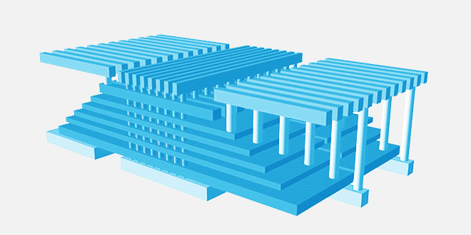
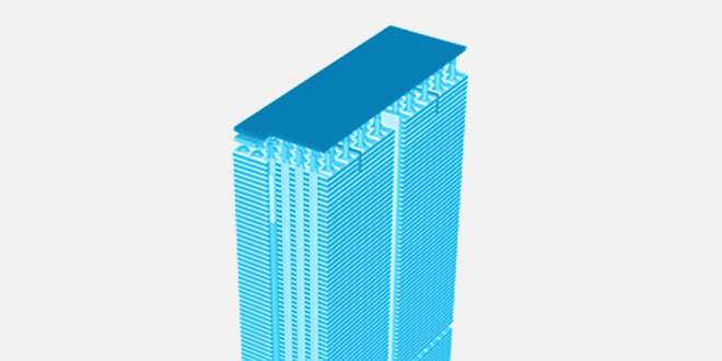
In 2007, KIOXIA announced the world’s first 3D flash memory technology, which was subsequently commercialized as “BiCS FLASH™.”
In addition, the development of Solid State Drive (SSD) became full-fledged. After having commercialized SLC NAND-embedded SSDs in 2001, we succeeded in commercialization of client SSDs with flash memory that incorporates multi-level cell technology in the late 2000s. SSDs have come to replace HDDs in notebook PCs, and have greatly contributed to high performance and light-weight notebook PCs.
|
2000 |
|
|---|---|
|
2001 |
|
|
2002 |
|
|
2003 |
|
|
2004 |
|
|
2005 |
|
|
2007 |
|
|
2008 |
|
|
2009 |
|
Column: Smartphones and Flash Memory
The advent of smartphones have changed the world for everyday life and the way we do business, and now is indispensable for our lives. One of the reasons smartphones have become popular is the feature to take photos and videos. Flash memory is also used to record photos and videos.
With improvement of quality of image, storage capacity of smartphones have increased each year, and now some smartphones have 1TB of storage per device. However, even if we need more storage, we cannot size up our smartphone. Thus flash memory is necessary to be placed in a limited space.
Through the development of various technologies, flash memory achieved large capacity and high performance, and supports the large storage of smartphones.

2010s
Flash memory from 2D to 3D
After the world’s first announcement of 3D flash memory technology in 2007, mass-produced products were also switched from 2D NAND flash memory to 3D flash memory (BiCS FLASH™) in the mid-2010s. The market for flash memory expanded in achieving more large-capacity memory products.
The market of SSD expanded from mobile PC products to servers and data centers along with the popularization of the Internet and the cloud, which began in the 2000s. Having acquired a lot of storage technologies and product know-hows in the enterprise and data center fields that require high performance and reliability, KIOXIA commercialized enterprise and data center products.
|
2010 |
|
|---|---|
|
2011 |
|
|
2012 |
|
|
2013 |
|
|
2014 |
|
|
2015 |
|
|
2016 |
|
|
2017 |
|
|
2018 |
|
|
2019 |
|
Column: SSD
SSD stands for Solid State Drive, which uses flash memory as storage medium. SSDs have advantage of high speed, low power consumption and shock resistance compared to Hard Disk Drives (HDDs) which use magnetic disks, but they were initially more expensive than HDDs and that was disadvantageous.
As the cost per bit was lowered by flash memory-intensive technology, we entered a market where we can leverage characteristics of SSDs such as faster PC boot-ups and low power consumption resulting in less heat generation, and users have enjoyed these benefits.

2020 and beyond
Creating a New Market as a Leading Company of Flash Memory and SSDs
Flash memory, which was first developed more than 30 years ago, was then 4Mbit per chip, 10,000 to 100,000 times more expensive than HDDs. After subsequent technology developments and cost reductions, flash memory has been used in products that have changed the society significantly, such as digital cameras, portable music players, smartphones, and SSDs.
KIOXIA’s flash memory and SSDs continue to evolve.
|
2020 |
|
|---|---|
|
2021 |
|
|
2022 |
|
|
2023 |
|
|
2024 |
|
|
2025 |
|
Column: The future of SSDs
As big data and IoT continue to increase, the amount of data handled by both businesses and individuals has increased exponentially. And the capacity and performance of the latest SSDs are exponentially improved, and the capacity of a single computer node being unexpendable. Sharing SSDs across the network is an urgent challenge.
A “software-defined storage solution” has emerged as an approach to solving this challenge. KumoScale™ developed by KIOXIA use a software layer to efficiently manage physical data storage capacity on a server, maximizing the performance of SSDs and thus flash memory.
KIOXIA continues to develop new applications and new markets that are based on flash memory, and that can only be achieved with flash memory.

Explanation of abbreviations
- SLC: Single Level Cell
- MLC: Multi Level Cell
- TLC: Triple Level Cell
- QLC: Quad Level Cell
- PATA: Parallel ATA, Parallel Advanced Technology Attachment
- SATA: Serial ATA, Serial Advanced Technology Attachment
- mSATA: mini SATA
- SAS: Serial Attached SCSI (Small Computer System Interface)

KIOXIA has been highly commended for the presentation of its R&D through a variety of channels, including major academic societies and research papers.

A technical glossary that covers terms related to KIOXIA products and technologies, such as memory and SSDs. We explain that it can be used by engineers and researchers to the general public.
Yokkaichi Plant is a a cutting-edge manufacturing site for flash memory products. Working with the R&D division adjacent to the plant, we promote the manufacture of highly-efficient, cutting-edge products.
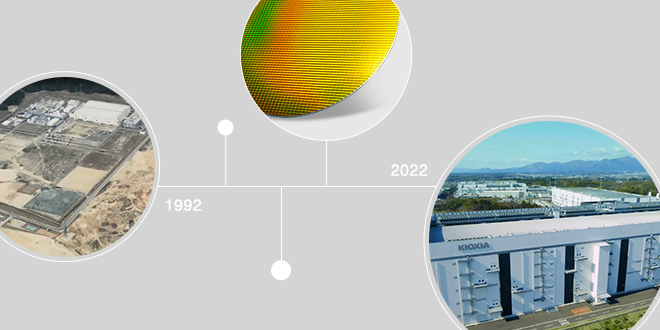
Yokkaichi Plant was established in 1992 and developed as a state-of-the-art semiconductor memory manufacturing facility.