Please select your location and preferred language where available.
What is Multi-level Cell Technology Realizing Larger Capacity Flash Memory?
“Multi-level cell technology” is one of the main technologies realizing larger capacity flash memory. The 1 Gbit MLC NAND flash memory launched by KIOXIA in 2001 was the first application in the world of multi-level cell technology to a NAND flash memory product.
The determination of “1” and “0” and data read/write operation on flash memory
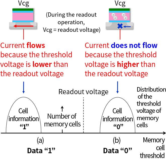
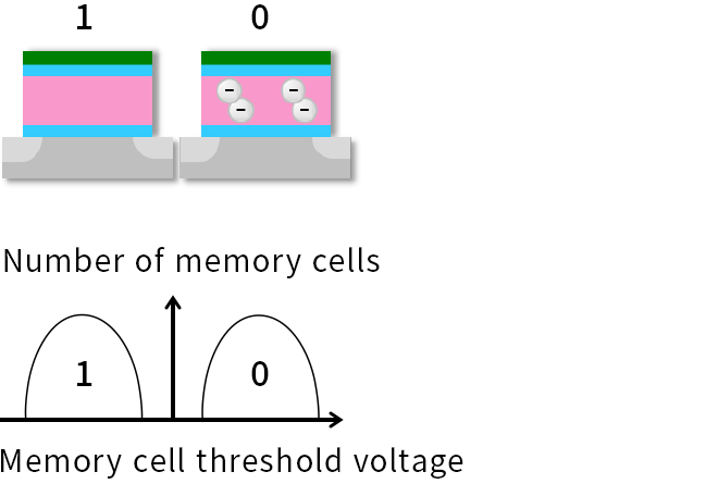
In flash memory, either “1” or “0” is stored depending on whether current flows in the memory cell. In addition, the higher the memory cell control gate voltage (Vcg) is, the easier it is for current to flow. The lower limit for the control gate voltage for which a current will flow is called the “threshold voltage.”
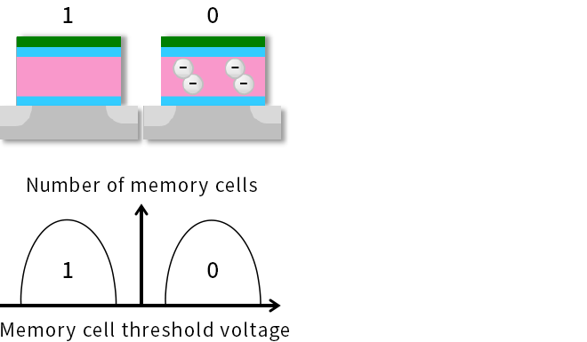
The lower the number of electrons in the charge storage film is, the easier it is for current to flow. For this reason, in the memory cell in Figure 1(a), the threshold voltage is lower because there are no electrons in the charge storage film. On the other hand, in the memory cell in (b), the threshold voltage is higher because there are many electrons in the charge storage film.
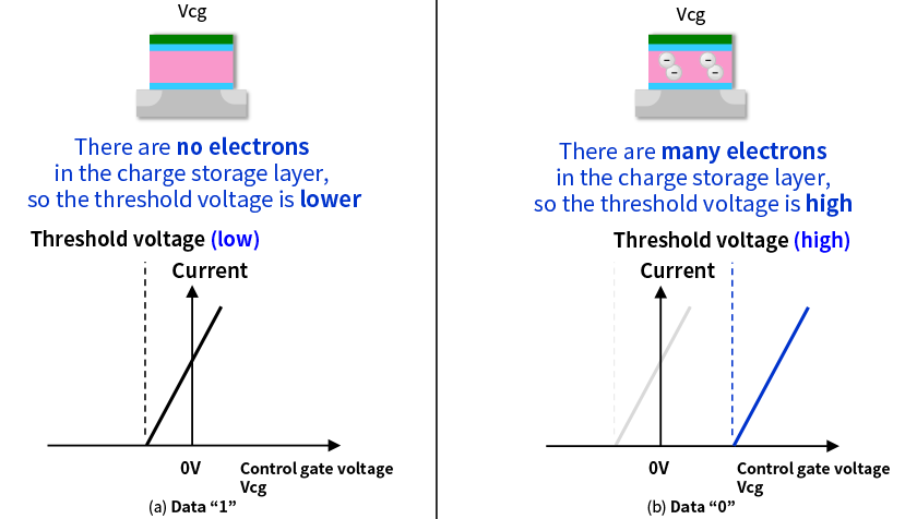
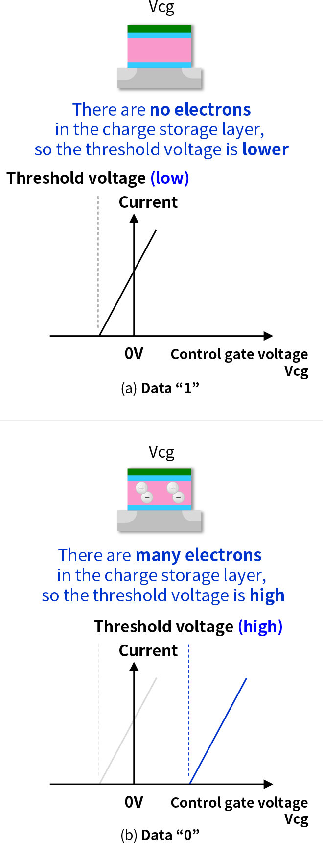
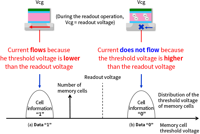
In the state where current is flowing easily, that is, the state where the threshold voltage is low, the data is “1”. Also, in the state where it is difficult for current to flow, that is, the state where the threshold voltage is high, the data is “0”. On an actual flash memory chip, there are an extremely large number of memory cells and even if they have the same data, there will be a difference in the threshold voltage for each memory cell, so the threshold voltages for “1” memory cells are distributed as shown in Figure 2(a). In the same way, the threshold voltages for “0” memory cells are distributed as shown in Figure 2(b).
During the read operation, the memory cell control gate voltage Vcg is set to the readout voltage, which is between the threshold voltage distribution for data “1” and the threshold voltage distribution for data “0”. At this time, in the data “1” memory cells, the threshold voltage is lower than the readout voltage, so current flows. In the data “0” memory cells, the threshold voltage is higher than the readout voltage, so no current flows.
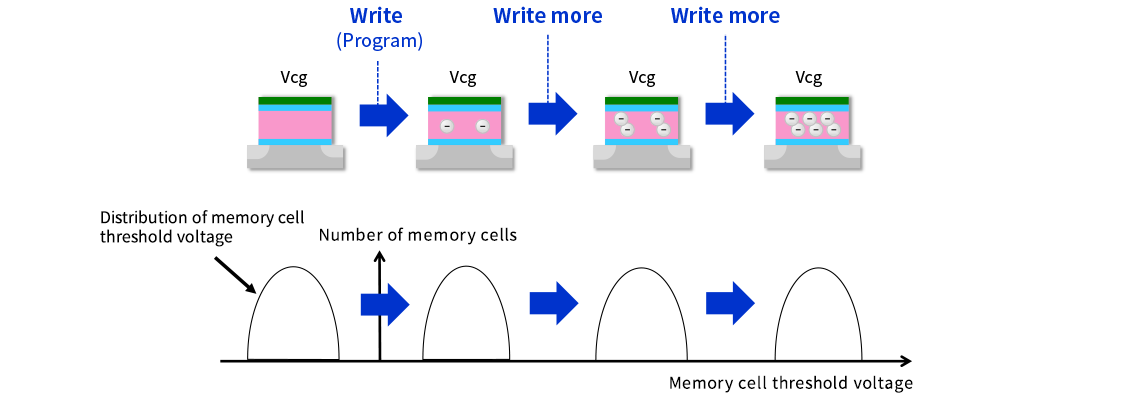
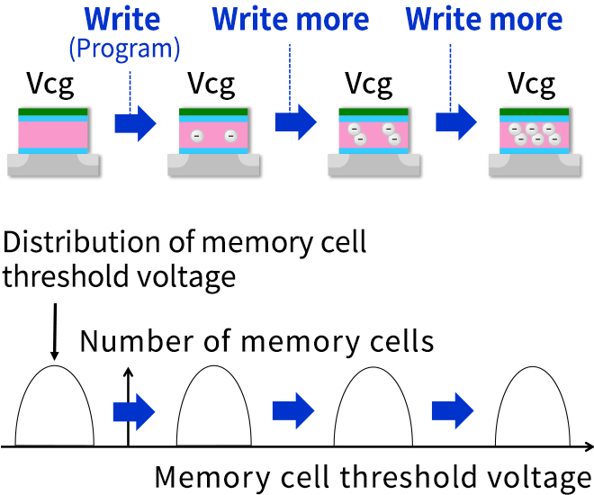
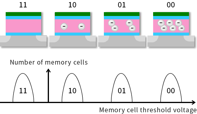
In flash memory, a write operation can change the threshold voltage of a memory cell. As shown in Figure 3, as the write operation is repeated, the number of electrons in the charge storage film in the memory cell increases and the threshold voltage increases.
Mechanism of capacity increases through multi-level cell technology
KIOXIA also realizes increased flash memory capacity with methods other than the “multilayering” on BiCS FLASH™. One of those methods is “multi-level cell technology.”
“Multilayering” can increase the number of memory cells per unit area by stacking them. On the other hand, with “multi-level cell technology,” it is possible to increase the amount of data that can be stored in each individual memory cell.
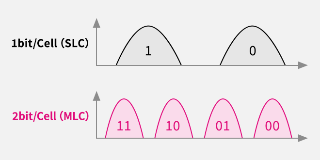
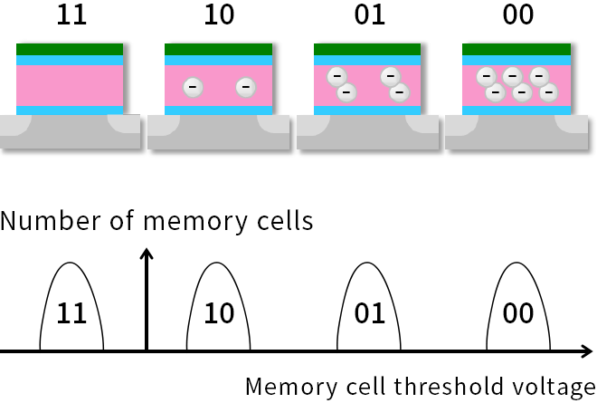
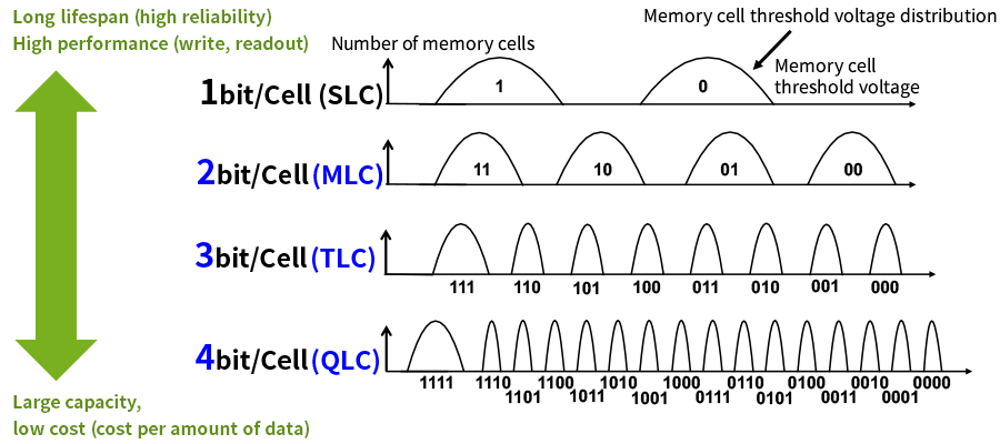
The units for the amount of data processed by a computer are called bits, where “1 bit” indicates the minimum amount of data that can be represented by a binary number. In a conventional memory cell, where a single memory cell stores a single bit, the two patterns of either “1” or “0” were stored. This corresponds to the “1 bit/Cell (SLC)” in Figure 4. As shown in Figure 3, by further subdividing the number of electrons in the charge storage film of a memory cell, it is possible to create more than three threshold voltage distributions. For example, if it is possible to create four threshold voltage distributions, then, as is shown in “2 bit/Cell (MLC)” in Figure 4, it is possible to express each of the threshold voltage distributions with a combination of “0” and “1”, so the four patterns of “11”, “10”, “01” and “00” can be stored. In this case, it is possible to store two bits of data in a single memory cell. Similarly, if it is possible to create eight threshold voltage distributions, then, as is shown in “3 bit/Cell (TLC)” in Figure 4, it is possible to store eight different patterns and three bits of data can be stored in a single memory cell.
Explanation of abbreviations
SLC: Single Level Cell, MLC: Multi Level Cell, TLC: Triple Level Cell, QLC: Quad Level Cell
1 bit/Cell (SLC): One bit of data is stored in a single memory cell
2 bit/Cell (MLC): Two bits of data are stored in a single memory cell
3 bit/Cell (TLC): Three bits of data are stored in a single memory cell
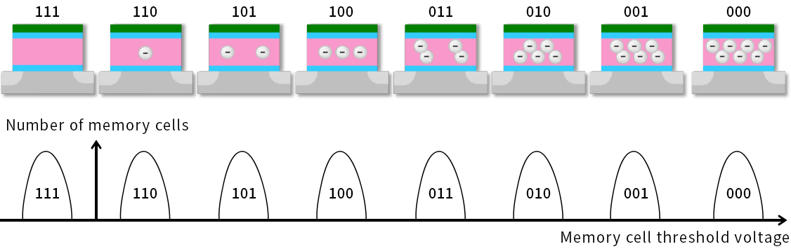
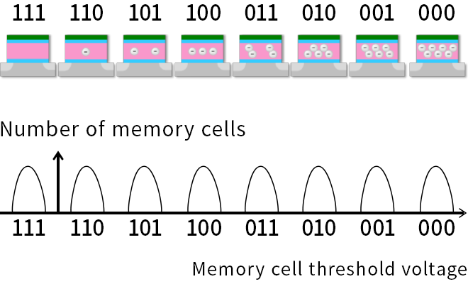
Figure 4. Multi-level cell technology for flash memory
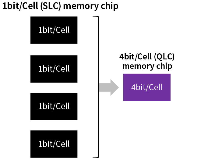
Furthermore, if it is possible to create 16 threshold voltage distributions, then, as is shown in “4 bit/Cell (QLC)” in Figure 5, it is possible to store 16 different patterns and four bits of data can be stored in a single cell. In this way, when the amount of data in a single memory cell is N bits, the number of threshold voltage distributions and the number of different patterns is 2 to the power of N.
Using different multi-level cell technology for different uses
If a number of bit N that is storage capacity per memory cell in flash memory increases with multi-level cell technology, the capacity of the flash memory can be increased and the cost per amount of data can be reduced. However, if increase the number of N, the finer threshold value distribution is required. For this, it is necessary to perform the writing slowly. Also, as the number of N increases, the intervals between the threshold voltages are narrower, so it is necessary to perform the readout slowly and the lifespan is shorter compared to when the number of N is small. In other words, larger N values are more suited to applications where capacity and cost are a priority, and smaller N values are more suited to applications where performance and longevity are a priority. This option to use different bit storage capacities per memory cell in the flash memory to suit different product applications has advantage that flash memories are used in an extremely wide range of applications.
Even if the write and readout are performed slowly, it is not easy to reduce the width of the memory cell threshold voltage distribution. In particular, to make the memory cell threshold distribution width and threshold distribution intervals extremely small as in the QLC shown in Figure 5, the technical difficulty is very high and it also is necessary to take on the challenge of increasing the performance and extending the lifespan as much as possible. For objectives such as these, an extremely high level of multi-level cell technology such as QLC is realized by bringing together technologies from a wide range of sectors such as circuit, process and manufacturing technology.
Explanation of abbreviations
SLC: Single Level Cell, MLC: Multi Level Cell, TLC: Triple Level Cell, QLC: Quad Level Cell
Multi-level memory chips to increase the memory capacity mounted
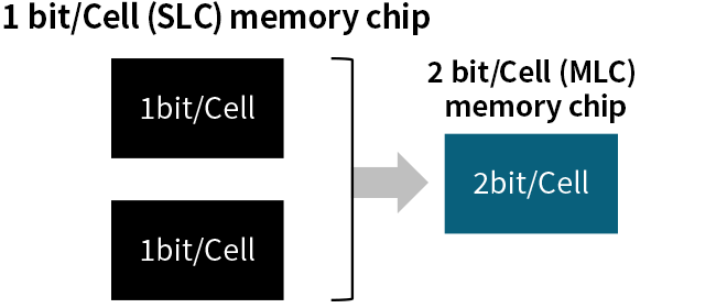
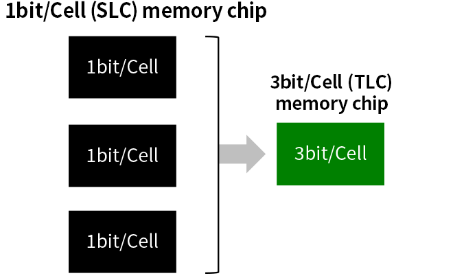
When the multi-level cell technology explained so far is used, it is possible to realize the capacity of multiple SLC memory chips with a single multi-level memory chip. As shown in Figure 6, this means, for example, that a product that previously needed the capacity of two SLC memory chips can be realized with a single MLC memory chip. Likewise, a product that required the capacity of three SLC memory chips can be realized with a single TLC memory chip, and a product that required four SLC memory chips can be realized with a single QLC memory chip.
When it is possible to reduce the number of memory chips to realize the same capacity, this means that some products will be able to increase the upper limit for their capacity. For example, in products where various parts are inserted into an extremely small space, such as on a smartphone or memory card, the capacity mounted is often determined by the space. However, even if the space available is the same, multi-level cell technology can be used to more than double the capacity mounted.
KIOXIA has been developing the multi-level cell technology described here since the Toshiba era. In 2001, we launched the 1 Gbit MLC NAND flash memory which was the first application in the world of multi-level cell technology to a NAND flash memory product. At an international academic conference in 2007, we presented the 16 Gbit QLC NAND flash memory which was the first application in the world of QLC technology to a NAND flash memory product.
- The figure is a simplified mechanism of “Multi-level cell technology” and may differ from the actual product.
KIOXIA memory and storage solutions enable the success of emerging applications and allow existing technologies to reach their expected potential.

We offer solutions built with our latest technology to take your digital experience to the next level. For peace of mind, KIOXIA memory cards, USB flash drives and SSD products feature reliability and quality, and are all backed by supportive customer service.
KIOXIA is one of the world’s largest flash memory suppliers, delivering a wide range of memory and SSD solutions that features innovative BiCS FLASH™ 3D Technology, to address next-generation storage applications for customers worldwide.