Please select your location and preferred language where available.
Frontier Technology R&D Institute
We aim to pursue continuous technological exploration and its social implementation to achieve an affluent and sustainable digitalized society through innovative memory technologies.
Frontier Technology R&D Institute will promote research and development of technologies to support the accelerated expansion of AI technology and its applications, high-capacity and high-speed memory system technologies utilizing new principles and new materials, and new process technologies to spread these technologies to society at low cost.
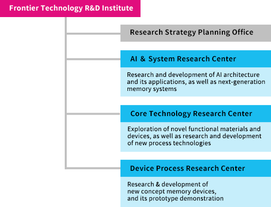
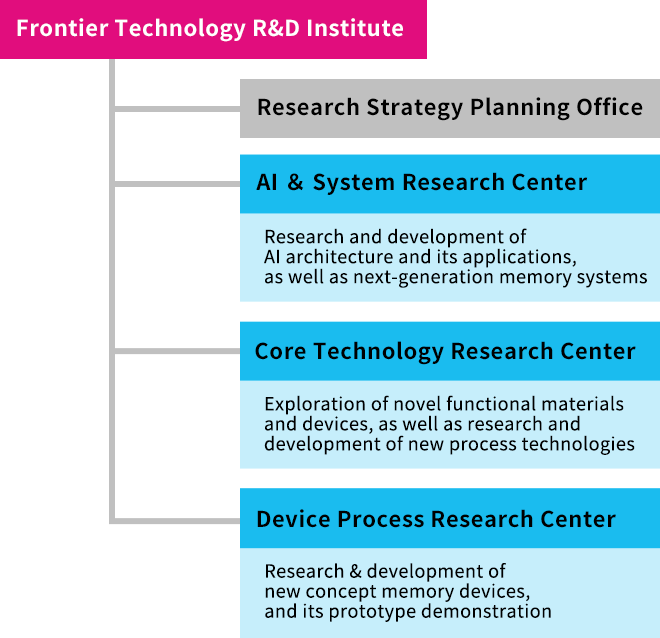
AI & System Research Center
AI & System Research Center is established with three core domains: “AI technology”, “device and circuit design technology”, and “system technology”. These core technology areas cooperate and combine with each other to consistently conduct new application exploration, designing, characterization and system development in a data-centric computing society.
With the accelerated growth of AI technology, data utilization becomes more important. Accordingly, the requirements for semiconductor memory and storage are dramatically changing to higher capacity, higher performance and lower power consumption. To meet the various needs, it is necessary to promote research and development with understanding the entire process from stand-alone device technology to marketing.
Through leading-edge development of AI and memory system technologies we will clarify the characteristics required for new semiconductor devices in advance, and apply them to circuit designing, evaluation and prediction of array-level and system-level performance effectively. Furthermore, we will promote research and development of core system technologies such as controllers, software, and hardware architectures that utilize new semiconductor devices with high performance and efficiency.
We will enhance the value of our products, and also provide new value to our customers.


Core Technology Research Center
Creation of new memory concepts is the most important mission in the Core Technology Research Center. To achieve higher memory capacity, higher performance, and new memory products of high value, it is important to continuously create world-leading new memory concepts in a timely manner. For achieving this great goal, we focus on research and development of new materials, processes and prototype devices based on new structures, by utilizing the clean room located at the Shin-Koyasu Technology Front.
We utilize computational science such as TCAD and first-principles calculations as well as fundamental technologies such as high-precision electrical characterization and advanced physical analysis toward development of new materials and devices based on physics. We also promote open innovation and cooperative research with universities, research institutes and device and material manufacturers.
After a proof-of-concept of a promising new memory technologies, we develop a product prototype with the 300mm fabrication line in collaboration with the Device Process Research Center in Yokkaichi, to bring a valuable new memory product to market.


Device Process Research Center
The Device Process Research Center conducts research and development of world-class device, process and integration technologies.
Next-generation memory products require advanced device technologies such as high-functional memory cells with new materials and structures, high-performance transistors for memory peripheral circuits, low-resistance contacts and nanoscale interconnection. In addition, a variety of process technologies are needed to fabricate devices on a 300mm silicon wafer, including lithography for ultra-fine patterning, etching processes and CMP to precisely process patterns, oxidation and deposition (CVD, ALD, sputtering) techniques to accurately form ultra-thin films of various materials. Finally, integration technology is required to achieve new device structures by skillfully linking above processes.
We will deliver new memory products that meet market demand by developing product prototypes that combine innovative device, process, and integration technologies.


Introducing the latest technologies being researched and developed at KIOXIA Corporation and various use cases of flash memories.
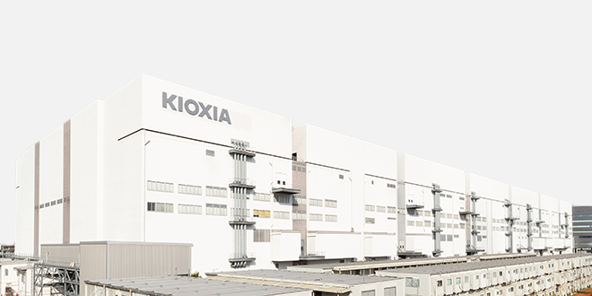
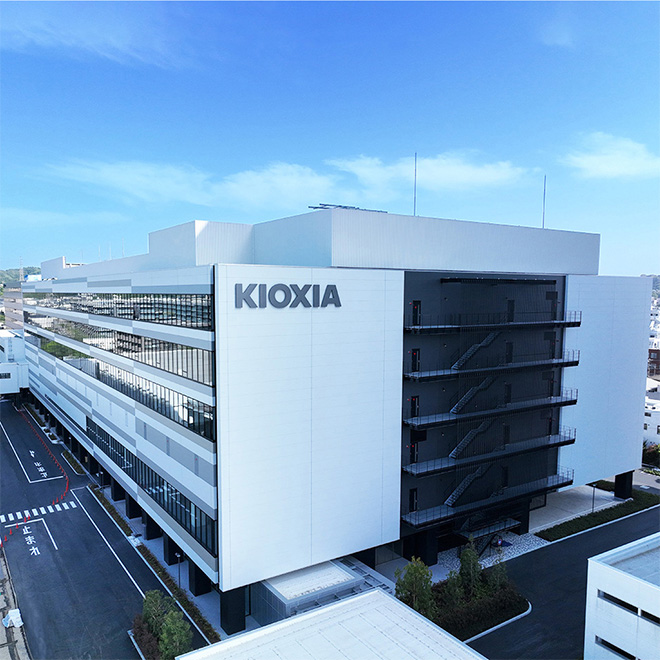
Yokkaichi Plant is a a cutting-edge manufacturing site for flash memory products. Working with the R&D division adjacent to the plant, we promote the manufacture of highly-efficient, cutting-edge products.