Please select your location and preferred language where available.
Technology Topics
Introducing the latest technologies being researched and developed at KIOXIA Corporation and various use cases of flash memories.
-
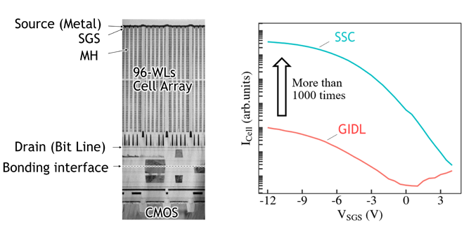
As the number of word lines increases in 3D flash memory, erase speed degradation is expected to become a significant issue. In this work, we propose a novel Schottky source junction that drastically enhances erase operation. The proposed structure was experimentally demonstrated using a prototype cell array. These results were presented at the 2025 IEEE Symposium on VLSI Technology and Circuits.
-
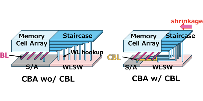
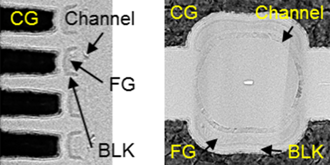
By adopting CBL(Crossed Bit Line) Architecture which is compatible with the CBA(CMOS directly Bonded to Array) technology in BiCS FLASH™ 8th generation, we achieved a 12% reduction in chip size. With the employment of CBL, we improved the sense amplifier operation. Furthermore, the adoption of OPS(On Pitch SGD) leaded to a 15% reduction in memory array area and a 4% reduction in read current.
-
BiCS FLASH™ generation 10 is high memory density 3D flash memory which is well-scaled to 29Gb/mm2 with 332 world-lines stacked and our layout optimization technique, and it achieved the highest bit density and smallest chip in the 1Tb products. We also realized 4.8Gbps data transfer rate and 29% improvement on read energy consumption with new Interface circuit and read operation method.
-
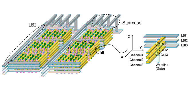
We proposed the new architecture, Horizontal channel flash, which enables further cost reduction for future 3D flash memory. We also examined its cell characteristics and confirmed 10k cycle program/erase operations on a test device. This achievement was presented at the IEDM 2024.
-
Metal-induced Lateral Crystallization (MILC) is a crucial technology for the high-stacking 3D flash memory. In this study, MILC mechanism was revealed at the atomic scale by using first-principles calculations. This achievement was presented at the international conference SISPAD 2024.
-
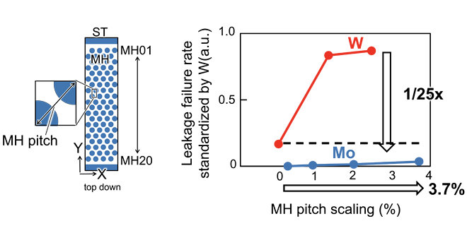
A state-of-the-art fluorine-free word line (WL) molybdenum (Mo) process has been established for future 3D flash memory. Application of Mo to WLs can accelerate scaling of cells in both the vertical and horizontal directions with lower RC delay and lower leakage failure rates compared to traditional tungsten. These results were presented at VLSI 2024.
-
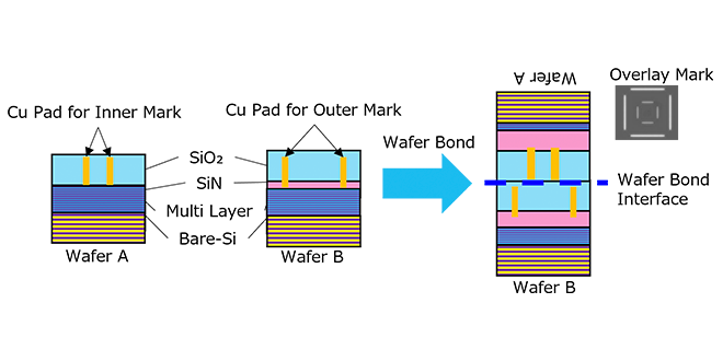
We demonstrated high-precision bonding overlay control techniques using a newly developed overlay measurement tool that uses infrared (IR) light. The accuracy of the IR-light overlay measurement was verified by using a conventional visible-light tool after silicon grind. The results show an excellent correlation between the bonding overlay and overlay after Si grind.
-
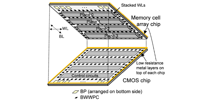
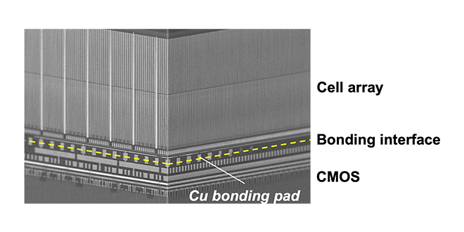
BiCS FLASH™ generation 8 is our latest high performance and high memory density 3D flash memory. Data are transferred to outside with 3.2Gbps speed, while data are read and programmed inside with 40μs time and 205MB/s throughput, respectively. The memory density of the 1Tb TLC product is well-scaled to 18.3Gb/mm2. We here introduce the two new technologies applied in order to enhance performance and the memory density: CBA (CMOS directly Bonded to Array) and OPS (On Pitch SGD).
-
CMOS directly bonded to array(CBA) technology with Cu direct bonding process has been developed and applied to BiCS FLASH™ generation 8 for performance improvement and cost reduction of 3D flash memory.
-
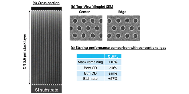
Memory hole etching of 3D flash memory devices requires high throughput and a well-controlled hole profile. Here, we summarize our new etching technology using a novel, environmentally friendly C3HF5 gas. These results were presented at the international DPS2023 conference.
-
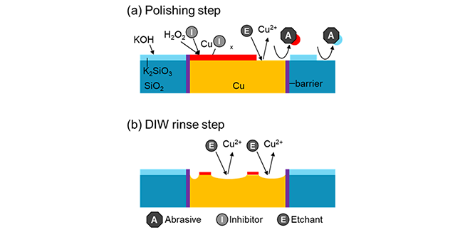
We investigated the dishing reduction of Cu bonding pads in the CMOS directly Bonded to Array(CBA) process, a new architecture for 3D flash memory. We found that the suppression of chemical etching during CMP can reduce dishing and improve yield. These results were presented at the international conference ICPT 2023.
-
The crystallization technology for Si channel, using metal-assisted materials, has been developed for 3D (three-dimensional) flash memory. It has successfully achieved cell array operation for the first time. This approach can reduce the density of grain boundaries in the Si channel, leading to reduction in trap density in Si channel compared to conventional polycrystalline Si channel. As a result, this technology can realize lower channel resistance, smaller RTN (random telegraphic noise) and narrower threshold voltage distribution in QLC (quadruple level cell) operation.
-
Large program/erase window, tight Vth distributions and superior data retention characteristics, which were essential to achieve multiple bits per cell, realized by optimizing read operation and FG structures in split-gate cells.
-
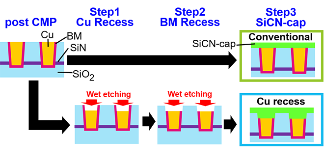
Highly reliable copper interconnect technology is required for the high-voltage circuits of 3D flash memory. We have developed Cu recess interconnect structure and demonstrated that this structure can improve Cu line-to-line reliability.
-
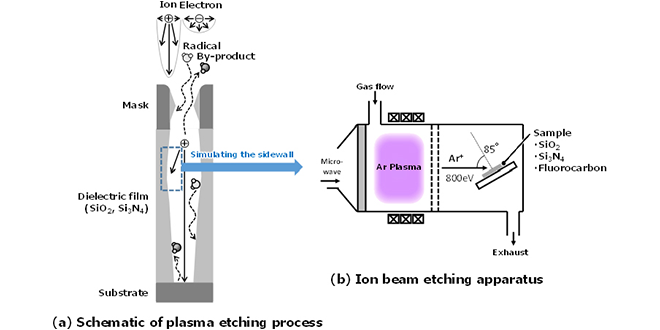
Understanding process mechanisms is critical for the development of next-generation BiCS FLASH™. We describe an example using memory hole etching, which is key to designing the memory cell.
-
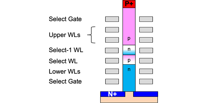
BiCS FLASH™ can increase its memory density and reduce the product cost by increasing the number of word line (WL) layers. The thyristor structure is one of the promising candidates to obtain a large read current even the number of stacked layers is increased.
-
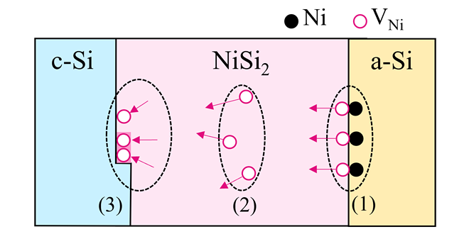
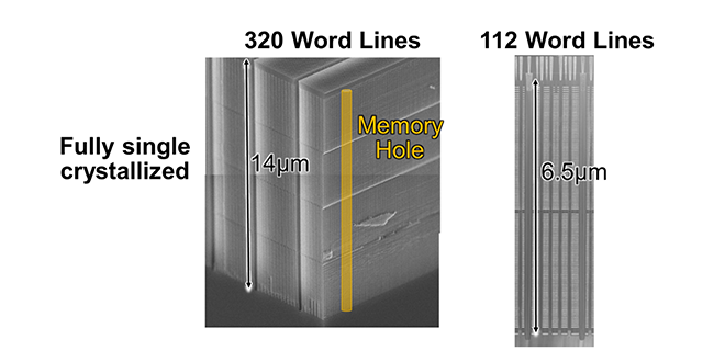
By applying MILC(Metal-induced Lateral Crystallization) technology to Si film in the vertical memory holes, we successfully fabricated the formation of monocrystalline Si from amorphous Si via nickel silicide.
The 3D flash memory cell devices equipped with this technology demonstrated superior electrical characteristics and reduced variation compared to conventional devices using poly-Si as the channel.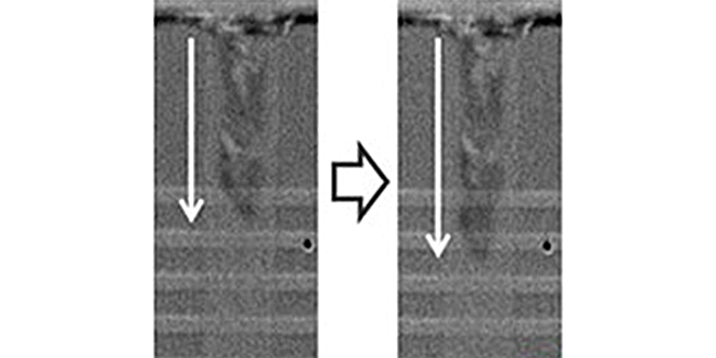
-
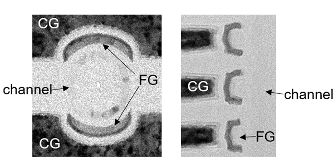
Three-dimensional (3D) semicircular split-gate flash memory cells have been successfully developed for the first time.
-
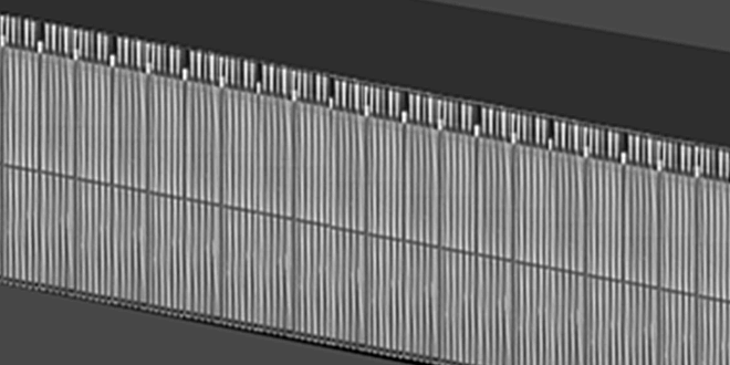
BiCS FLASH™ 3D flash memories, electrode and dielectric layers are alternately stacked all at once, and then holes are punched through all the layers at once, to reduce the number of manufacturing processes. For these manufacturing processes, plasma etching (RIE: Reactive Ion Etching) technology is crucial in order to form deep memory holes with a uniform diameter.
-
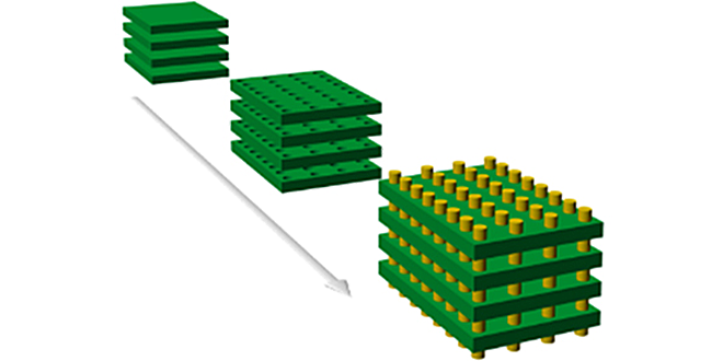
To meet the demand for ever-smaller, higher-capacity storage devices, it is essential to increase the storage density of flash memories. For two-dimensional (2D) NAND flash memories, we have employed nanofabrication and other technologies to develop a 15-nm memory cell, realizing such flash memories. However, geometry scaling is approaching the physical limit. BiCS FLASH™ overcomes the density limit through multilayer cell array stacking.
R&D Organization

We aim to pursue continuous technological exploration and its social implementation to achieve an affluent and sustainable digitalized society through innovative memory technologies.
Conducts R&D on BiCS FLASH™, a type of 3D flash memory that KIOXIA was the first to develop in the world, while serving as a bridge between R&D and volume production.

KIOXIA memory and storage solutions enable the success of emerging applications and allow existing technologies to reach their expected potential.

A technical glossary that covers terms related to KIOXIA products and technologies, such as memory and SSDs. We explain that it can be used by engineers and researchers to the general public.

KIOXIA has established industry-leading R&D frameworks with “memory” technology. We use our various locations to conduct technological innovation while promoting open innovation.