Please select your location and preferred language where available.
Development of a 1Tb 3b/Cell BiCS FLASH™ generation10 product
June 18, 2025
We presented the development of a 1Tb 3b/Cell BiCS FLASH™ generation10 product at the international conference ISSCC2025. This product is developed by Kioxia Corporation and Sandisk Corporation, it is high memory density 3D flash memory which is well-scaled to 29Gb/mm2 with 332 world-lines stacked and our layout optimization technique, and it achieved the highest bit density and smallest chip size in the 1Tb products. In addition to introducing Toggle DDR 6.0, our new Interface(IF) circuit and read operation method realized 4.8Gbps data transfer rate and 29% improvement on read energy consumption. The following are brief introductions from three technical perspectives.
Layout technique
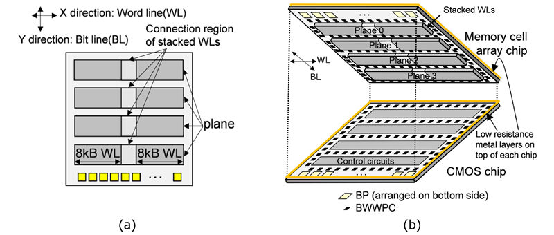
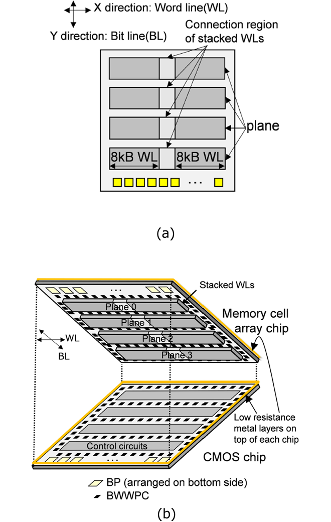
This product has introduced CBA (CMOS directly Bonded to Array) architecture as same as conventional product. However, four planes are arranged in vertical direction[1] which is different from before product. This floorplan makes Bonding Pad (BP) area reduction, and it enables the reduction of the overhang area by half[1] (Figure 1(a)). As shown in Figure 1(b), the lowest sheet resistance layers are applied to top metal layer of Memory cell array chip and CMOS chip, and those layers are effectively connected with BWWPC[1] (Bonding pads for Wafer-to-Wafer Power Connection). This strong power network leads high area efficiency with circuits compaction, and improvement of circuit performance.
Interface technique
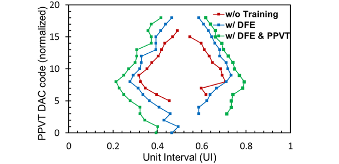
IF architecture with Unmatched DQS is shown in Figure 2(a). Per Pin VREF Training(PPVT) for using optimal reference for input receiver of each DQ and 2-way Time Interleaved - Decision-Feedback Equalizer(2TI-DFE) with Data-Driven Self-Reset (DDSR) circuit are newly adopted. The schematic of 2TI-DFE with DDSR is shown in Figure 2(b), and the timing chart is shown in Figure 2(c). 4TI-DFE is well-known technique in DRAM interfaces for improving data input margin while it needs 4 sense-amplifier (S/A) circuits for each DQ, and it leads to energy consumption and area overhead increase. In this product DDSR circuit is newly introduced, it can retain decisions, OPO、OMO, until 1PE and 1ME change, as detected by the 3-input NAND gate, which avoids the feedback error[1]. As a result, we realized reducing the energy consumption and area overhead by reducing the number of interleaved[1] DFE from 4 to 2.
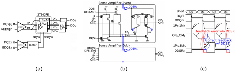
Figure 3 shows a shmoo plot for all the DQ[7:0]. We confirmed 2TI-DFE and PPVT make a contribution to 4.8Gbps data transfer rate.
CORE Read performance improvement technique
As a consequent of highly stacked WLs, the charging of unselected WLs is the dominant factor that increases Read time (tRead) and current consumption[1] in Read operation. To solve these problems in continuous Reads, we have applied WL voltage-swing reduction control which is shown in Figure 4. In conventional continuous reads the unselected WL voltage changes between VSS and the read voltage level (Vread), which is generated by a charge pump[1]. In this work after a reading from the first WL, we discharge VREAD down to an intermediate potential, which is higher than VSS. Then we charge up from this intermediate potential to VREAD for the next read[1]. It is possible to reduce Vread set-up time and current consumption of the next Read operation due to the smaller voltage-swing for unselected WLs.
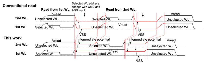
Fig.4 Operational waveforms ©2025 IEEE
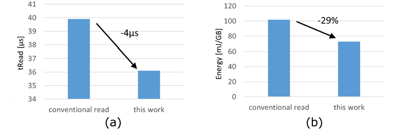
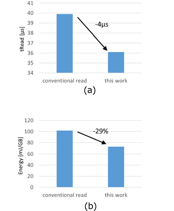
Figure 5(a) shows that our proposed scheme reduces tRead by 4μs, corresponding to a 10% improvement[1]. Figure 5(b) shows the read energy efficiency, where a notable 29% improvement is achieved[1].
We have succeeded in developing an area- and energy-efficient 3D flash memory[1] which has introduced layout optimization technique with highly stacked WLs and high-speed interface and low power circuit design technique. We contribute to provide a high performance and high-capacity flash memory and continue circuit design with making an effort to reduce power consumption more at the same time.
This achievement was presented at the ISSCC 2025.
Reference
[1] K. Yanagidaira et al., “30.2 A 1Tb 3b/cell 3D Flash Memory with a 29%-Improved-Energy-Efficiency Read Operation and 4.8Gb/s Power-Isolated Low-Tapped-Termination I/Os,” ISSCC, pp506-507, 2025. © 2025 IEEE

A technical glossary that covers terms related to KIOXIA products and technologies, such as memory and SSDs. We explain that it can be used by engineers and researchers to the general public.

KIOXIA has established industry-leading R&D frameworks with “memory” technology. We use our various locations to conduct technological innovation while promoting open innovation.