Please select your location and preferred language where available.
Improvement of Line-to-line Reliability by Cu Recess Interconnect Structure
October 19, 2022
3D flash memory is facing increasing demands for higher capacity, lower bit cost, and higher speed. In order to realize these requirements, in addition to the requirement of fine pitch and low resistance, highly reliable interconnect structure is necessary at the same time. The reason why higher reliability is required for interconnects than for other semiconductor devices such as SoC (system on chip) and DRAM (dynamic random access memory) is that 3D flash memory requires high-voltage circuits to control the memory cells.
Copper (Cu), which has lower resistance than conventional tungsten, is a promising interconnect material candidate and is being developed for introduction. To realize higher Cu line-to-line reliability, it is important to suppress drift of Cu ions (Cu2+) through the trap site or defect site at the interface of SiCN cap layer and SiO2 inter layer dielectrics (ILD). We have developed Cu recess interconnect structure that selectively etched Cu line from the interface of SiCN cap and SiO2 ILD. Also, we demonstrated that this structure can improve Cu line-to-line reliability.
Figure 1 shows cross-sectional schematic image of process procedure. Damascene trench reactive ion etching (RIE) was carried out after lithography in SiO2 ILD and SiN etch stop layer. Then, barrier metal (BM) and Cu were filled into the trench, and Cu and BM chemical mechanical polishing (CMP) was processed. Cu recess interconnect structure is realized with additional wet etching processes.
Table 1 shows cross-sectional transmission electron microscope (TEM) and energy dispersive X-ray spectroscopy (EDS) mapping images. On conventional Cu interconnect structure has flat Cu and BM surface with the interface of SiCN cap/SiO2 ILD. On the other hand, both Cu and BM were clearly recessed from the interface of SiCN cap/SiO2 ILD on Cu recess interconnect structure.
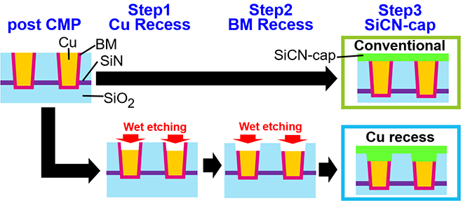
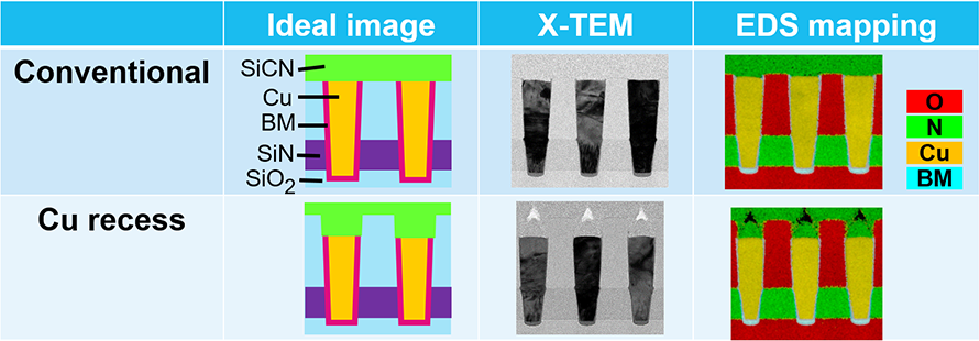
Figure 2 shows the results of time dependent dielectric breakdown (TDDB) test. On Cu recess interconnect structure, mean time failure (MTF) has significantly improved compared to conventional Cu interconnect structure.
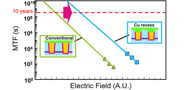
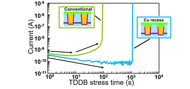
Figure 3 shows leakage current as a function of TDDB stress time. On conventional Cu interconnect structure, leakage current decreases initially due to electron trapping and then gradually increases due to the drift of Cu2+ or other cations, then broke down. On the other hand, Cu recess interconnect structure showed leakage current continued to be decreased due to electron trapping by the time of breakdown.
These results indicate that the Cu recess interconnect structure suppresses Cu2+ drift through the trap site or defect site at the interface of SiCN cap layer and SiO2 ILD, thereby improving Cu line-to-line reliability. Thus, Cu recess interconnect structure is promising structure for both higher capacity, lower bit cost, and higher speed 3D flash memory.
This work was presented in the International Interconnect Technology Conference 2022 (IITC 2022) in Jun. 2022 [1].
Reference
[1] Mitsuhiko Noda et al., "Improvement of Line-to-line TDDB by Cu and Barrier-metal Recess Structure for high voltage circuit in 3D Flash Memory," 2022 IEEE International Interconnect Technology Conference (IITC), 2022, pp. 45-47, doi: 10.1109/IITC52079.2022.9881298.

A technical glossary that covers terms related to KIOXIA products and technologies, such as memory and SSDs. We explain that it can be used by engineers and researchers to the general public.

KIOXIA has established industry-leading R&D frameworks with “memory” technology. We use our various locations to conduct technological innovation while promoting open innovation.