Please select your location and preferred language where available.
Schottky Source Contact for Enhancing Erase Operation of 3D Flash Memory with Over 1,000 Word Lines
September 18, 2025
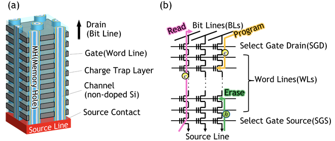
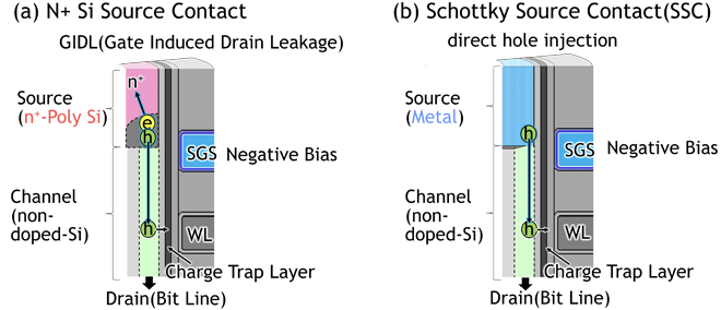
As shown in Figure 1, a typical 3D flash memory performs program operation by injecting electrons supplied from the drain into the charge trap layer of the memory cell, and erase operation by injecting holes supplied from the source. During read operation, electrons flow from the source to the drain. To increase cell density, the number of stacked word lines (WLs) in the cell array needs to be increased. However, as the number of WLs increases, more electrons and holes need to be supplied to ensure reliable cell performance.
Copyright (2025) The Japan Society of Applied Physics[2]
However, in the conventional N+-Si source contact, holes for erase operation must be generated by GIDL (Gate Induced Drain Leakage) because holes do not exist at the N+-Si source, which results in the degradation of erase speed as the number of WLs increases. To address this issue, we proposed and developed a novel SSC (Schottky source contact) structure and experimentally demonstrated its cell operation.
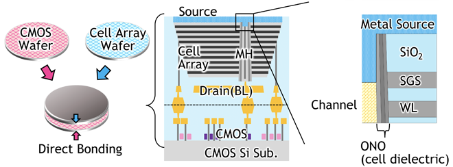
We successfully developed and are now manufacturing 3D flash memory with a CMOS Directly Bonded to Array (CBA) structure, where CMOS circuits and memory cells are fabricated on separate wafers and interconnected by wafer bonding [1]. The SSC structure is formed by depositing a metal layer onto the cell array surface of the CBA structure, which has been flipped through the bonding process, thereby creating a Schottky junction between the metal and the intrinsic Si channel (Figure 2).
Copyright (2025) The Japan Society of Applied Physics[2]
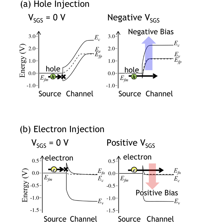
However, by applying negative and positive electric fields, corresponding to electron and hole injection respectively, from the select gate source (SGS) located adjacent to the junction structure, separated by a cell dielectric layer, ohmic contacts for both electrons and holes can be achieved.
Copyright (2025) The Japan Society of Applied Physics[2]
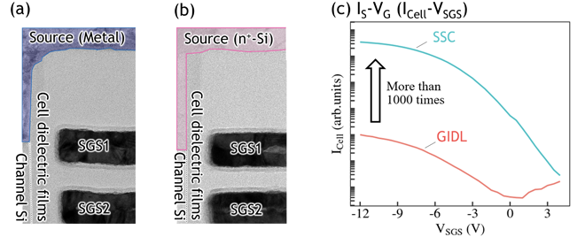
The SSC structure allows the supply of both electrons and holes from the source. This ambipolar characteristic enables improved erase speed without any degradation of cell characteristics compared to the conventional N+-Si source (Figure 4).
Copyright (2025) The Japan Society of Applied Physics[2]
To verify the fundamental operation of the SSC structure, we fabricated a cell Test Element Group (TEG), as shown in Figure 3(a). Evaluation of the erase current revealed that the SSC structure achieves a hole current more than 1000 times greater than that of the conventional N+-Si source structure.
Copyright (2025) The Japan Society of Applied Physics[2]
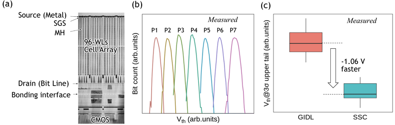
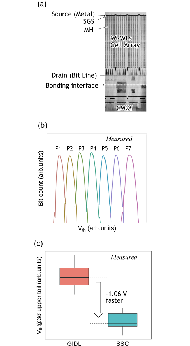
In order to evaluate cell array characteristics, we developed a 96-WLs 3D flash memory with a CBA structure incorporating the SSC structure, and successfully demonstrated program operation with 3 bit per cell. Furthermore, comparison of threshold voltage distributions during the erase operation confirmed that applying the SSC structure improves erase speed.
Copyright (2025) The Japan Society of Applied Physics[2]
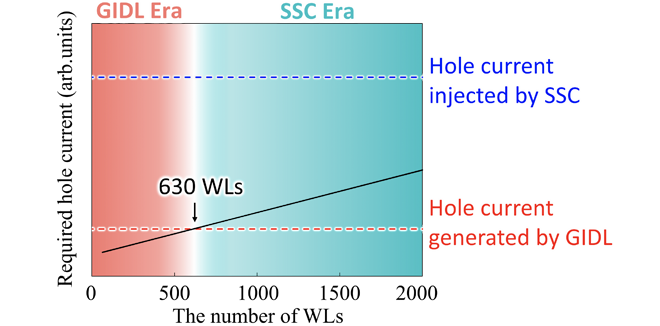
Based on these results, we estimated the trend of the required hole current for the erase operation (Figure 7). In the conventional N+-Si source structure, erase speed degradation begins at around 630 WLs, whereas the SSC structure can supply sufficient hole current even beyond 1000 WLs. The SSC structure is expected to be a breakthrough technology that enables reliable erase operation in future 3D flash memory with an extremely high number of word lines.
Copyright (2025) The Japan Society of Applied Physics[2]
This achievement was presented in the 2025 Symposium on VLSI Technology and Circuits [2].
Reference
[1] Masayoshi Tagami, “CMOS Directly Bonded to Array (CBA) Technology for Future 3D Flash Memory”, 2023 IEEE International Electron Devices Meeting (IEDM).
[2] Susumu Hashimoto et al., “A Schottky junction as a hole injector for enhancing erase operation of 3D flash memory in CMOS Directly Bonded to Array (CBA) era with over 1,000 word lines”, 2025 IEEE Symposium on VLSI Technology and Circuits, T9-1.

A technical glossary that covers terms related to KIOXIA products and technologies, such as memory and SSDs. We explain that it can be used by engineers and researchers to the general public.

KIOXIA has established industry-leading R&D frameworks with “memory” technology. We use our various locations to conduct technological innovation while promoting open innovation.