Please select your location and preferred language where available.
3D Semicircular Flash Memory Cell (Twin BiCS FLASH)
Novel Split-Gate Technology to Boost Bit Density
January 10, 2020
Three-dimensional (3D) semicircular split-gate flash memory cells have been successfully developed for the first time. Properly designed semicircular Floating Gate (FG) cells achieve superior program slope and program/erase window at much smaller cell size relative to circular Charge Trap (CT) cells. It is projected that the semicircular split-gate FG cell is a promising candidate to realize more than four bits/cell (QLC) for significantly higher memory density at a lower number of stacking layers.
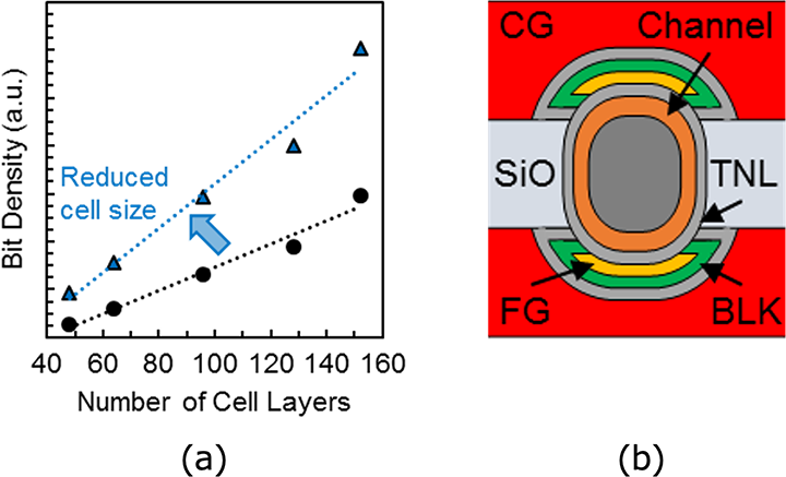
3D flash memory technology has realized high bit density with low cost per bit by increasing the number of cell stacks and implementing multilayer stack deposition and high aspect ratio etch [1]. In recent years, as the number of cell layers is exceeding 100 [2], managing the fundamental trade-offs among etch profile control, size uniformity and productivity is becoming increasingly challenging. This work demonstrates the 3D semicircular split-gate cell technology that attains a considerable reduction in cell size with significant gains in the program slope and program/erase window compared to the conventional circular cell, enabling higher-density memories at the lower number of cell layers (Fig. 1).
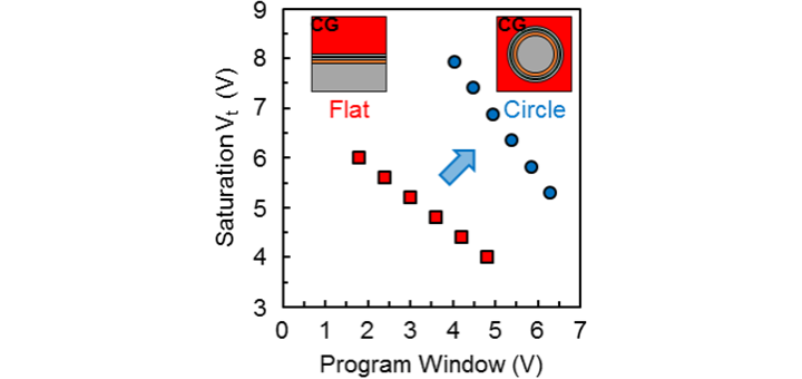
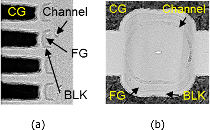
The circle-shaped control gate provides larger program window with relaxed saturation problems when compared with a flat-shaped gate because of the curvature effect [3], where carrier injection through the tunnel dielectric is enhanced while electron leakage to the block (BLK) dielectric is lowered (Fig. 2). In this split-gate cell design, the circular control gate is symmetrically divided into two semicircular gates to take advantage of the strong improvement in the program/erase dynamics. As shown in (Fig. 3), the conductive storage layer is employed for high charge trapping efficiency in conjunction with the high-k BLK dielectrics, achieving high coupling ratio to gain program window as well as reduced electron leakage from the FG, thus relieving the saturation issue. The FG is completely isolated for each cell, which eliminates charge migration across adjacent cells.
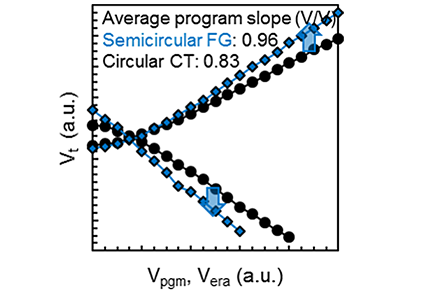
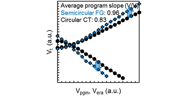
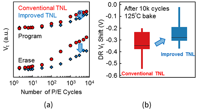
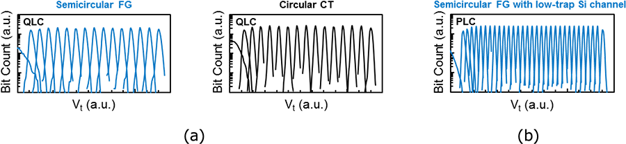
The experimental program/erase characteristics in (Fig. 4) reveal that the semicircular FG cells with the high-k-based BLK exhibit higher program slope and larger program/erase window over the larger-sized circular CT cells. Furthermore, careful tailoring of TNL film quality and interface formation processes sufficiently improves endurance and post-cycling data retention up to 10k cycling stress (Fig. 5). The semicircular FG cells, having superior program/erase characteristics, are expected to attain comparably tight QLC Vt distributions at small cell size, and integration of low-trap Si channel is capable of more than four bits/cell, e.g., Penta-Level Cell (PLC) as projected in (Fig. 6). These results confirm that the semicircular FG cell is a viable candidate for advancing the quest to boost bit density.
The novel split-gate structure, in which the control gate of the conventional circular cell is divided into the semicircular shape, demonstrates the large number of bits/cell at significantly reduced cell size, therefore providing high bit density with the low number of cell stacks. We will continue to refine the cell design/characteristics and pursue research and development toward practical applications.
[1] H. Tanaka, et al., “Bit cost scalable technology with punch and plug process for ultra high density flash memory”, Symp. VLSI Tech. Dig., p. 14, 2007.
[2] C. Siau, et al., “A 512Gb 3-bit/cell 3D flash memory on 128-wordline-layer with 132MB/s write performance featuring circuit-under-array technology”, ISSCC Tech. Dig., p. 218, 2019.
[3] S. Amoroso, et al., “Semi-analytical model for the transient operation of gate-all-around charge-trap memories”, IEEE Trans. Electron Devices, p. 3116, 2011.

A technical glossary that covers terms related to KIOXIA products and technologies, such as memory and SSDs. We explain that it can be used by engineers and researchers to the general public.

KIOXIA has established industry-leading R&D frameworks with “memory” technology. We use our various locations to conduct technological innovation while promoting open innovation.