Please select your location and preferred language where available.
Crossed Bit Line(CBL) Architecture in 3D Flash Memory CMOS Directly Bonded to Array(CBA) Structure
August 26, 2025
BiCS FLASH™ 8th generation adopted CBA(CMOS directly Bonded to Array) technology[1], which involves fabricating CMOS circuit and memory array on separate silicon wafers and then bonding them together. This technology offers two benefits: improved operating speed and reduced chip size. The improvement in operating speed is achieved by optimizing the thermal process for CMOS circuit and memory array formation separately. This article introduces the CBL(Crossed Bit Line) architecture, which contributes to the second benefit, the reduction of chip size, and the technique for improving sense amplifier operating margins and the effects of the OPS(On Pitch SGD) technology[2].
In the conventional CUA(CMOS Under Array) structure, the BLs(Bit Lines) are placed above the memory array, while the S/As(Sense Amplifiers) which control BLs, are placed below the memory cells. Therefore, an area called TAP is needed to place contact holes to connect the BLs to the S/As. In the CBA structure, on the other hand, BLs on the memory array chip and S/A on the CMOS chip are arranged facing each other after wafer bonding. This eliminates the TAP region for the connection between BL and S/A, thereby reducing the chip size (Figure 1).
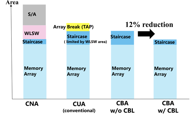
Next, we explain the area reduction of WL(Word Line) hookup area called the Staircase. The width of WLSW(Word Line Switch), which is the WL driver circuit, is usually wider than the Staircase width due to ensuring the transistor performance and inter-device breakdown voltage. In conventional architecture, since the width of the S/A matches that of memory array, so this causes WLSW to be extended beyond the Staircase. In other words, Staircase has to be expanded to the width of the WLSW. This causes an increase in chip size, consequently higher costs. Therefore, as shown in Figure 2, we reduce S/A width less than memory array width and push WLSW under the memory array. This allows the Staircase to be formed at its original width, thus reducing the chip size. However, this approach causes a misalignment between S/A position and their corresponding BL. To resolve this issue, we employed CBL which are oriented orthogonally to the BL to establish connections BL to their respective S/A.
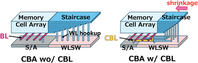
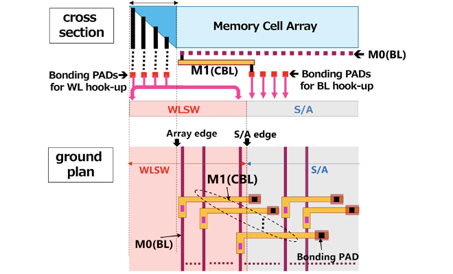
The CBL wiring drawn to the S/A position is connected to the S/A on the CMOS chip via the bonding pad. In addition, a portion of the WLSW is placed under the memory array, which causes wiring congestion between the WLSW and the Staircase. To resolve this, we used the three wiring layers on the CMOS chip and successfully placed all WLSWs under the Staircase and memory array (Figure 3). This CBL architecture can optimize the S/A and WLSW placement and it leads to the reduction of the Staircase width. We achieved a 12% reduction in chip size in BiCS FLASH™ 8th generation[2] (Figure 1).
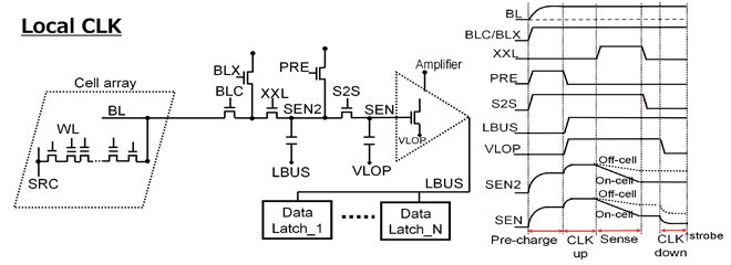
When placing all WLSWs under the Staircase and the memory array by implementing CBL architecture, it’s necessary to reduce the S/A width. However, if the number of wiring tracks within the pitch is reduced due to the S/A width shrink, it becomes difficult to maintain inter-wiring capacitance used for sense node. This results the degradation of the S/A operating margin. To overcome this challenge, the Local CLK method divides the conventional sense node into two part, SEN and SEN2 node, which are coupled to VLOP and LBUS respectively. A sufficient S/A operating margin was ensured by controlling these signals with optimal timing even with a smaller number of wiring tracks.
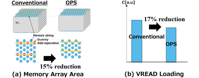
OPS technology is also employed as described in the article “Overview of new technologies applied to BiCS FLASH™ generation 8”. By eliminating the dummy memory strings which do not function as memory cells, we achieved a 15% reduction in the memory array size. Additionally, unselected WLs loading can be reduced by 17%, this leads to 1μs improvement of readout time and a 4% reduction in read current.
As we have introduced so far, CBL architecture and OPS are effective technologies for the continuous improvement of memory density and cost reduction in 3D flash memory. We will apply these technologies to our future products to enhance performance and develop products with higher memory density.
This achievement was presented at the IMW2025 (International Memory Workshop 2025).
Reference
[1] S. Kobayashi et al., “High Performance 3D Flash Memory with 3.2Gbps Interface and 205MB/s Program Throughput based on CBA(CMOS Directly Bonded to Array) Technology”, IEEE International Electron Devices Meeting (IEDM), Dec. 2023, 35-2.
[2] H.Maejima et al., “Crossed Bit Line (CBL) Architecture in 3D Flash Memory CMOS Directly Bonded to Array (CBA) Structure”, IEEE International Memory Workshop (IMW), pp.25-28, May.2025.

A technical glossary that covers terms related to KIOXIA products and technologies, such as memory and SSDs. We explain that it can be used by engineers and researchers to the general public.
KIOXIA has established industry-leading R&D frameworks with “memory” technology. We use our various locations to conduct technological innovation while promoting open innovation.