Please select your location and preferred language where available.
Optimal Cell Structure/Operation Design of 3D Semicircular Split-gate Cells for Ultra-high-density Flash Memory
November 9, 2022
Abstract
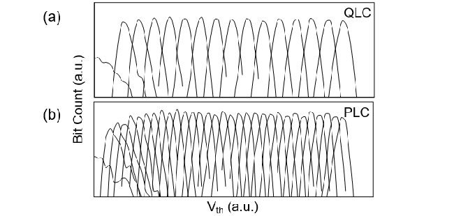
Three-dimensional (3D) semicircular split-gate floating-gate (FG) cells have been successfully developed for expanding the capability of multiple bits per cell. Large program/erase (P/E) window, tight Vth distributions and superior data retention characteristics were realized by optimizing read operation and FG structures. As a result, Vth distributions of four bits/cell (quadruple-level cell: QLC) and five bits/cell (penta-level cell : PLC) were experimentally demonstrated.
Introduction
3D flash memory technology has responded to the market demand for higher bit density with low cost and larger capability by increasing the number of cell stack layers [1]. Aggressive cell stacking structure is requiring multi-layer stack deposition and high aspect ratio etch. So the fundamental trade-offs among etch profile control, size uniformity and productivity have been severe. To overcome this issues, we proposed split-gate flash memory with semicircular FG cells (Twin BiCS FLASH) [2] and continued to refine the cell characteristics. Control gate (CG) split structure has several challenge such as leakage current of back-side cell, P/E window reduction due to parasitic leakage at gate-edge and random telegraph noise (RTN) increase due to smaller cell area. We overcome these challenges by optimizing read operation and cell structures and realize large P/E window, tight Vth distributions and superior data retention characteristics [3].
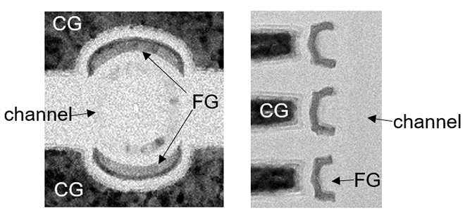
Optimization of cell operation to read Vth on both sides individually
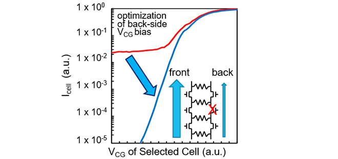
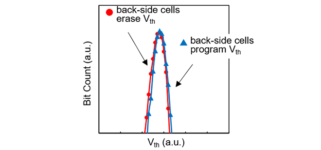
This split-gate cell has a structure in which FG and CG are divided while the channel is connected. Therefore, when reading a selected cell, leakage current through the channel of the back-side cell should be suppressed. By optimizing back-side gate bias, this leakage is cut-off and the current of selected cell have been obtained correctly, as shown in (Figure 2). By this optimization, Vth of selected cells can be read regardless of the state of the back-side cells (Figure 3).
FG Structure engineering for improvement of P/E window, Vth distributions and data retention
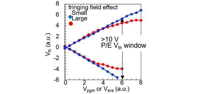
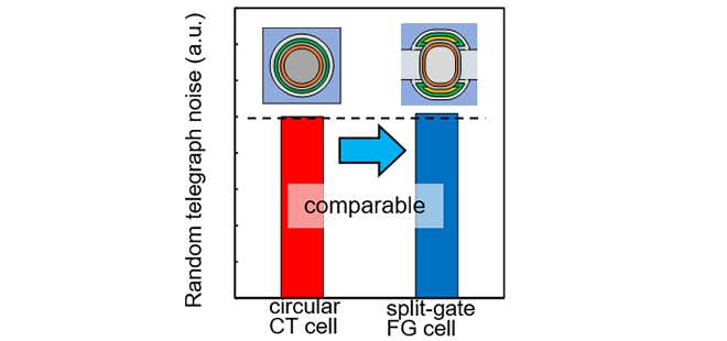
In the split-gate cell, reduction of parasitic leakage at gate-edge which caused by fringing field effect is essential to extract the maximum P/E window. This fringing field effect is suppressed by FG structure engineering, and large P/E window of more than 10 V is obtained as shown in (Figure 4). RTN increase due to cell size reduction is also challenge of split-gate cells, however adoption of FG makes RTN of small-size cell comparable to conventional circular charge trap (CT) cell (Figure 5)
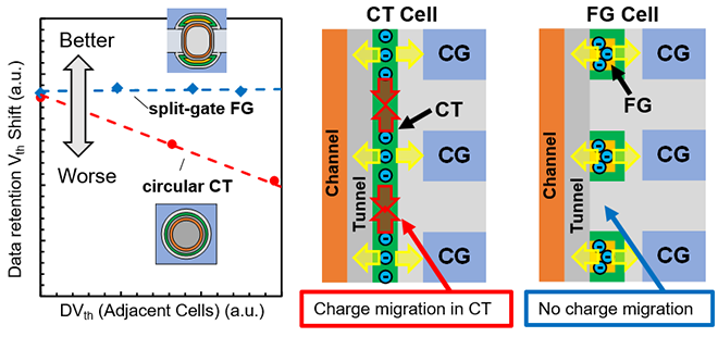
The FG in split-gate cells is completely isolated for each cells, so charge migration across adjacent cells is suppressed compare to CT cells. As a result, constant data retention characteristics is obtained regardless of the Vth difference with adjacent cells (Figure 6).
Demonstration of QLC and PLC Vth distributions
By optimizing the cell operation and structure, the distributions of QLC and PLC have been experimentally demonstrated by the split-gate cell arrays for the first time (Figure 7).
Summary
Twin BiCS FLASH, in which the control gate of the conventional circular cell is divided into the semicircular shape, can achieve both cell size reduction and multiple bits per cell. This cell structure is a promising candidate to boost bit density with minimum increase in stacking layer number.
This achievement was presented in the 2022 IEEE Symposium on VLSI Technology & Circuits [3].
This article is reconstructed from excerpts of references [3] @IEEE.
Reference
[1] H. Tanaka, et al., “Bit cost scalable technology with punch and plug process for ultra high density flash memory”, Symp. VLSI Tech. Dig., p. 14, 2007.
[2] M. Fujiwara, et al., “3D Semicircular Flash Memory Cell: Novel Split-Gate Technology to Boost Bit Density”, IEDM Tech. Dig., p. 642, 2019.
[3] T. Morooka et al., “Optimal Cell Structure/Operation Design of 3D Semicircular Split-gate Cells for Ultra-high-density Flash Memory”, Symp. VLSI Tech. Dig., p. 308-309, 2022.

A technical glossary that covers terms related to KIOXIA products and technologies, such as memory and SSDs. We explain that it can be used by engineers and researchers to the general public.

KIOXIA has established industry-leading R&D frameworks with “memory” technology. We use our various locations to conduct technological innovation while promoting open innovation.