Please select your location and preferred language where available.
Reliable memory cell operation in 64 Gbit cross-point MRAM
April 15, 2025
The recent rapid growth in emerging application demand, such as AI and big data processing, is changing the conventional memory hierarchy. Specifically, a new layer called storage-class memory (SCM) with high performance and low cost is expected to enable efficient computing.
STT-MRAM (Spin Transfer Torque Magnetic Random Access Memory), utilizing p-MTJ (perpendicular Magnetic Tunneling Junction) as the memory cell, is a promising candidate for next-generation non-volatile memory. Thanks to superior performance of MTJ, STT-MRAM has already entered the market in both embedded and standalone forms. However, transistors as select devices present challenges for increasing density. The 4 Gb STT-MRAM developed in collaboration with SK hynix in 2016 remains the largest capacity to date[1].
While MTJ technology has demonstrated high-speed operation and reliability, there have been several challenges in realizing high density MRAM. These challenges primarily include insufficient writing current provided by select transistors, the fabrication of MTJs with small size and narrow pitch, and reliable memory cell operation. To ensure sufficient writing current, we employed two terminal select devices instead of transistors and demonstrated basic cell operation in 2022[2].
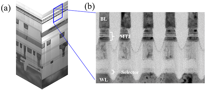
At IEDM 2024, we showcased advanced technologies to address the remaining two challenges[3]. Figure 1 shows (a) panoramic and (b) cross-sectional TEM images of the 64 Gb cross-point MRAM developed in collaboration with SK hynix. To achieve small and narrow-pitch MTJ fabrication, it is indispensable to co-optimize MTJ materials and the fabrication process. We successfully prevented electrical shorts between MTJs and wiring while avoiding MTJ property degradation, with MTJ diameter of 20 nm and half-pitch of 20.5 nm. This corresponds to the world’s smallest MRAM cell area of 0.001681 μm2.
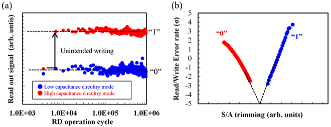
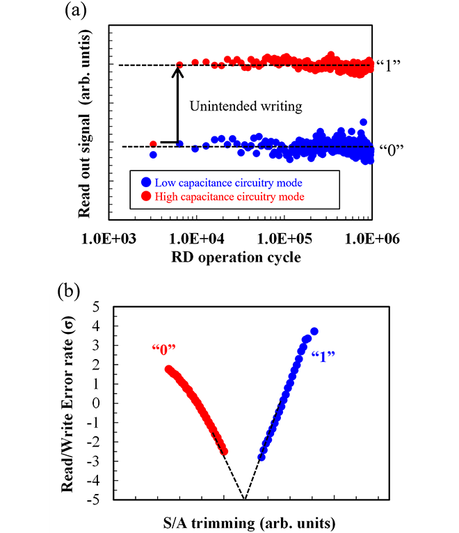
In conventional read methods, unintended writing occurs when the selector turns on, especially for small MTJs, leading to cell operation reliability degradation. We overcame this issue by utilizing the transient behavior of the selector along with a low-capacitance circuitry design. Figure 2(a) shows the cyclic read test for an MTJ initialized to the low-resistance state (“0”). When the high-capacitance circuitry mode (red dots) is applied, the MTJ rapidly switches to the high-resistance state (“1”). On the other hand, with the low-capacitance circuit mode (blue dots), the MTJ state does not change even after at least 1 million read operations.
Figure 2(b) shows the cyclic read/write operation test to assess the cell operation failure rate for a typical bit in a 64 Gb array. With the optimal circuitry setting, the failure rate achieves around -5σ (2.87e-07), demonstrating reliable cell operation.
These results pave the way for high-density MRAM, enabling high-performance and low-cost SCM applications.
This achievement was presented at the IEEE IEDM 2024.
Reference
[1] S.-W. Chung et al., “4Gbit density STT-MRAM using perpendicular MTJ realized with compact cell structure”, IEDM Tech. Digest, pp.659-662, 2016
[2] S.M. Seo et al., “First demonstration of full integration and characterization of 4F2 1S1M cells with 45 nm of pitch and 20 nm of MTJ size”, IEDM Tech. Digest, pp.218-221, 2022
[3] Hisanori Aikawa et al., “Reliable memory operation with low read disturb rate in the world smallest 1Selector-1MTJ cell for 64 Gb cross-point MRAM”,2024 International Electron Devices Meeting (IEDM), San Francisco, CA, USA, 10-1

A technical glossary that covers terms related to KIOXIA products and technologies, such as memory and SSDs. We explain that it can be used by engineers and researchers to the general public.

KIOXIA has established industry-leading R&D frameworks with “memory” technology. We use our various locations to conduct technological innovation while promoting open innovation.