Please select your location and preferred language where available.
World’s Highest Density 64Gbit MRAM with Novel Reading Technique for Highly Reliable Operation
May 27, 2025
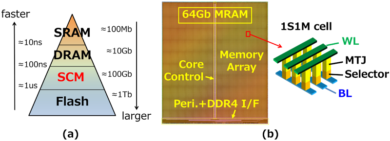
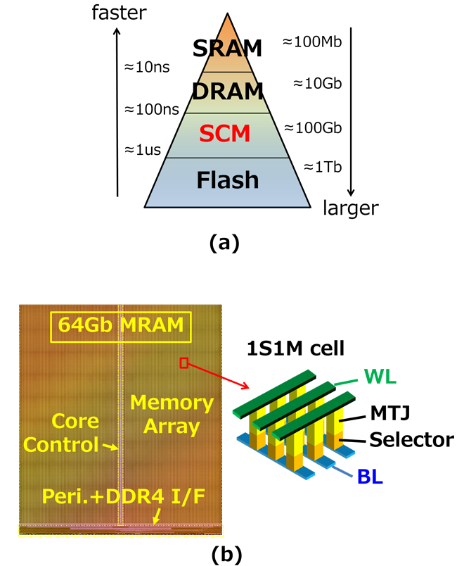
The introduction of storage class memory (SCM) is expected due to the increasing demand for high-capacity and high-speed operation of new applications (Figure 1(a)). We believe that MRAM based Magnetic Tunnel Junction (MTJ) is one of the candidate for SCM due to its high speed and reliability, but large-capacity MRAM for SCM application has not been developed so far [1]. In this work, we developed a 1S1M structure connecting MTJ and Selector in series to achieve a high-density (4F2) cell array [2-3] and implemented a 64Gb MRAM chip (Figure 1(b)).
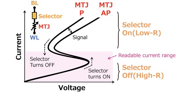
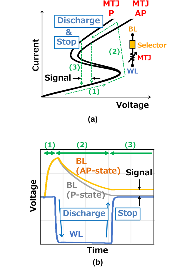
The MTJ has low resistance state (P) and high resistance state (AP) and the Selector functions as a switch with ON/OFF states (Figure 2). Typically, in resistance change memory devices, read signals is obtained from the current when a constant voltage is applied or from the voltage when a constant current is applied. However, when applying the same method in a 1S1M cell, issues such as oscillation of Selector ON/OFF states and disturbance of MTJ state (Read-Disturb), leading to low reading reliability.
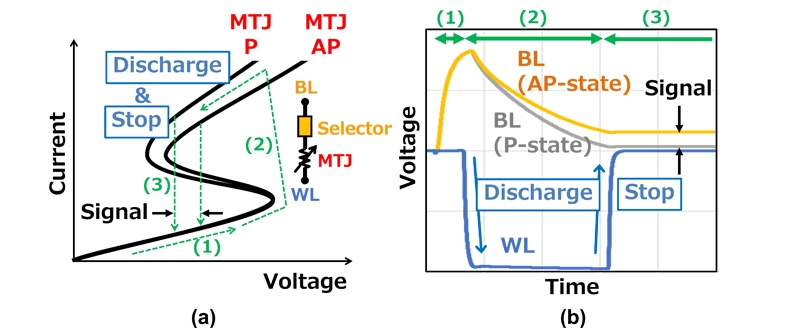
“Time-controlled-discharge reading scheme” can suppress read disturb and oscillation by controlling the ON timing of the selector while discharging (Figure 3). After charging the Bit-line (BL) with a constant voltage, the voltage of the Word-line (WL) is pulled down to discharge the voltage. The BL voltage is determined and read by the sense amplifier (S/A) when the selector transitions to the OFF state, allowing the MTJ state to be read with minimal current flowing through the MTJ.
To further address read disturb, we proposed “Local capacitance mode” (LC mode), which minimizes the parasitic capacitance of BL by inserting a transistor in BL, and reading by receiving the cell signal voltage at the gate for the transistor when the selector transitions to the OFF state, leading to reduction of the current flowing through the memory cell and faster discharge time (Figure 4).
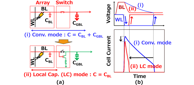
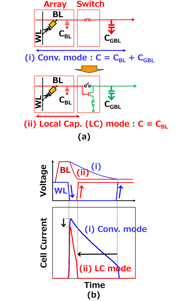
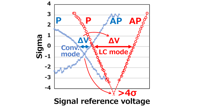
Figure 5 shows results of the distribution of read signal when applying reading pulses of a few-ns to the P/AP states of the MTJ on the 64Gb MRAM chip. By utilizing the proposed reading schemes, we demonstrated that the S/A reference voltage becomes P<AP within the >4σ range, achieving a high read margin at a practical level.
These results demonstrated that MRAM has potential to participate in new markets such as SCM applications and CXL system.
This achievement was presented at the ISSCC2025.
Reference
[1] K. Rho et al., “A 4Gb LPDDR2 STT-MRAM with compact 9F2 1T1MTJ cell and hierarchical bitline architecture”, ISSCC, pp. 396-397, 2017.
[2] S. M. Seo et al., “First demonstration of full integration and characterization of 4F2 1S1M cells with 45 nm of pitch and 20 nm of MTJ size”, IEDM, pp. 218-221, 2022.
[3] H. Aikawa et al, “Reliable memory operation with low read disturb rate in the world smallest 1Selector-1MTJ cell for 64 Gb cross-point MRAM”, IEDM, pp. 20.1.1-20.1.4, 2024.
[4] K. Hatsuda et al., “A 64Gb DDR4 STT-MRAM Using a Time-Controlled Discharge-Reading Scheme for a .001681um 1T-1MTJ Cross-Point Cell”, ISSCC, pp. 30.6.1-30.6.4, 2025.

A technical glossary that covers terms related to KIOXIA products and technologies, such as memory and SSDs. We explain that it can be used by engineers and researchers to the general public.

KIOXIA has established industry-leading R&D frameworks with “memory” technology. We use our various locations to conduct technological innovation while promoting open innovation.