Please select your location and preferred language where available.
Image processing technology utilizing machine learning
February 28, 2019
State-of-the-art semiconductor manufacturing requires highly accurate defect inspection even if the defects are very small. We are developing a new inspection technique utilizing not only conventional image processing but also machine learning.
The left-hand figure below shows an example of conventional defect inspection in the semiconductor manufacturing process using SEM (Scanning Electron Microscope). Defects such as open or short failure of metal wires on semiconductor wafer are detected by comparing with the CAD layout*1 of the circuit. But as the pattern transferred on a wafer is not identical to the CAD layout, excess detection of non-defects may occur. We have developed the novel inspection technique shown in the right-hand figure below. We apply machine learning to generate a virtual SEM image from the CAD layout and compare it with the SEM image to get more accurate results*2. We will continue to introduce advanced machine learning that progresses day by day and develop technologies that contribute to higher yields and higher quality of our products.
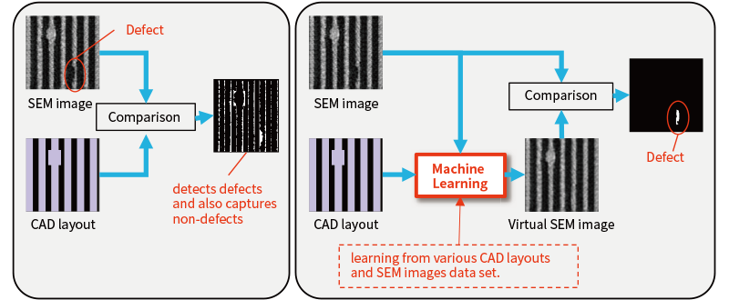
- CAD (Computer Aided Design) drawing for semiconductor IC manufacturing (e.g., wiring )
- Joint development with Toshiba Corp.

A technical glossary that covers terms related to KIOXIA products and technologies, such as memory and SSDs. We explain that it can be used by engineers and researchers to the general public.

KIOXIA has established industry-leading R&D frameworks with “memory” technology. We use our various locations to conduct technological innovation while promoting open innovation.