

Please select your location and preferred language where available.
UFS & e-MMC for Consumer & Industrial
Advanced Embedded Memory Solutions: Powering the Present and Future of Consumer and Industrial Applications
KIOXIA’s high-capacity UFS embedded flash memory devices integrate BiCS FLASH™ 3D flash memory and a controller in a single package. The built-in controller manages error correction, wear leveling, address translation, and bad block management, making system development easier, lowering processor demands, accelerating time to market, and improving usability.
Blazing Ahead: KIOXIA UFS 5.0 Sets a New Standard for Mobile Speed and Efficiency
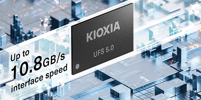
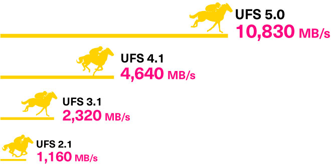
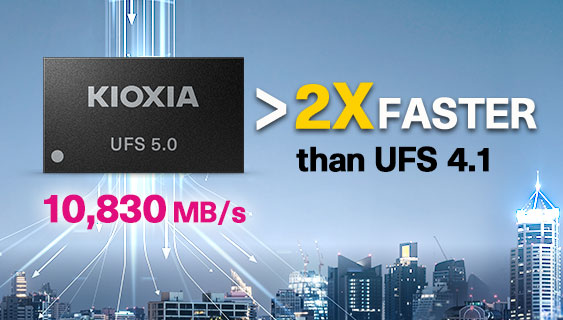
UFS 5.0 takes embedded storage technology to the next level, delivering even faster transfer speeds and improved power efficiency for future smartphones, tablets, and AI-powered mobile devices. Building upon the advancements of its predecessors, UFS 5.0 utilizes MIPI® M-PHY® version 6.0 High Speed Gear6 and UniPro® version 3.0, supporting theoretical interface speeds of up to 10.8GB/s(1) (10,830 MB/s) per device. UFS 5.0 maintains backward compatibility with UFS 4.1, ensuring seamless integration with existing platforms while delivering enhanced performance and support for the latest flash memory innovations.


Interview

New Era of On-device AI Driven by High-speed UFS 5.0 Storage
UFS 5.0, featuring a theoretical high-speed interface of 10.8 GB/s, is almost here. KIOXIA believes that the adoption of UFS 5.0 in smartphones will further advance on-device AI. This is because high-speed UFS 5.0, with high-capacity, will allow for the storage of Large Language Models (LLMs) and Retrieval-Augmented Generation (RAG) databases.
Key Features and Benefits of KIOXIA UFS 5.0
Key Features
- Serial interface
- Enhanced interface speed of up to 10.8GB/s per device(1)
- Latest JEDEC® standard
- Capacities: 512GB, 1TB(2)
- MIPI M-PHY version 6.0 High Speed Gear6
Impressive Performance
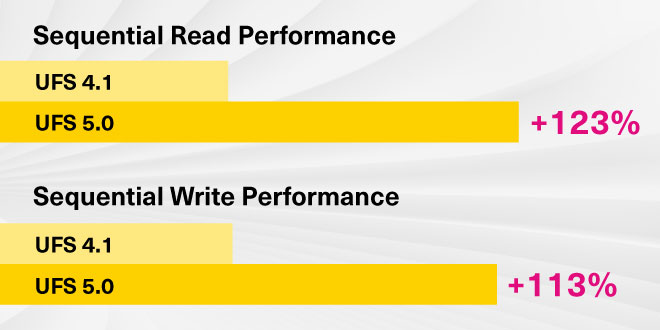
UFS 5.0 delivers significant performance improvements, with sequential read and write speeds increasing by up to 123% and 113% respectively over UFS 4.1 devices.(3)* This high performance is enabled by the High-Speed Gear6, which achieves its interface speeds via new technologies such as PAM-4.
* 1TB device, driver level performance vs. UFS 4.1 1TB

Enhanced Power Efficiency and Thermal Management
UFS 5.0 offers improved power efficiency and thermal management, reducing energy consumption when operating and heat generation for higher sustained performance compared to UFS 4.1.
UFS 5.0 vs UFS 4.1
KIOXIA offers both UFS 4.1 and the latest UFS 5.0 high-capacity flash memory solutions, each incorporating an integrated controller and advanced error correction. UFS technology simplifies system design by offloading storage management from the host processor and enabling easier integration.
UFS 5.0 introduces several enhancements over UFS 4.1, including:
- Faster interface speeds for higher data throughput
- Improved sequential and random read/write performance
- Greater energy efficiency to support demanding next-generation devices
These enhancements make UFS 5.0 well-suited for high-end mobile devices that will be able to support on-device AI due to UFS 5.0’s faster interface speeds.
Why KIOXIA UFS

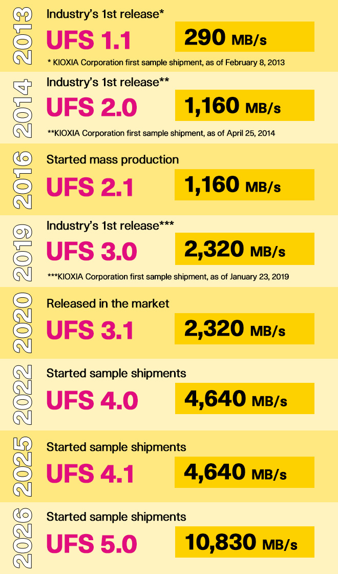
KIOXIA continues its legacy of innovation with the introduction its UFS 5.0 flash memory solutions, addressing the need for ever-increasing speed and efficiency in modern embedded storage. Building on years of technological leadership and a track record of industry firsts, KIOXIA UFS 5.0 solutions are engineered for demanding applications, like on-device AI in smartphones and other high-performance computing systems.
UFS 5.0 for Advanced Applications

The UFS 5.0 standard provides significant leaps in data transfer speeds, improved responsiveness, and further optimized power consumption. These features translate into seamless experiences—enabling rapid app loading, ultra-fast data downloads, and efficient multitasking for the most intensive mobile and embedded use cases.
As digital products evolve and require greater responsiveness and agility, KIOXIA UFS 5.0 flash memory helps manufacturers deliver the next wave of innovative user experiences with impressive performance improvements.(3)*
- Seqential Read: 10,000 MB/s +123%
- Sequential Write (WB): 9,000 MB/s +113%
- Random Read: 1,160 KIOPS +71%
- Random Write: 1,020 KIOPS +59%
* 1TB device, driver level performance vs. UFS 4.1 1TB
KIOXIA UFS Key Technology

PAM-4 Support**
PAM-4, or Pulse Amplitude Modulation with 4 levels, is a technology that allows devices to send more information in each signal by using four distinct signal strengths instead of just two. This approach effectively doubles the amount of data that can be transmitted without needing extra connections or wires. In UFS 5.0, PAM-4 enables much faster data transfer speeds. As a result, users experience quicker app launches, faster file transfers, and smoother performance, helping devices keep pace with the demands of modern apps, high-resolution media, and multitasking.
** Key technology to HS-Gear6 in UFS5.0 only

WriteBooster Functionality
WriteBooster enhances write performance by utilizing the existing user data area as a temporary SLC buffer without sacrificing capacity. Maximum SLC buffer size can be configured by the host at device configuration and the host can keep writing data to the buffer until the buffer is filled. This feature is enabled dynamically during operation by the host depending on system performance requiriements of 5G and other applications.

High Speed Link Startup Sequence (HS-LSS) support
With conventional UFS, Link Startup (M-PHY and UniPro initialization sequence) between device and host is performed at low-speed PWM-G1 (3~9Mbps***), but with HS-LSS, it can be performed at faster HS-G1 Rate A (1248Mbps). This is expected to reduce the time for Link Startup by approximately 70% compared to the conventional method.
*** PWM-G1 communication speed depends on the product.

Next-Generation 3D Flash Memory Technology
KIOXIA UFS 5.0 utilizes state-of-the-art BiCS FLASH™ 3D flash memory and introduces further controller optimizations, designed to maximize throughput, provide lower latency, and efficiently support the rigorous requirements of modern mobile, automotive, and enterprise devices.
KIOXIA UFS 5.0 Key Applications

High-end smartphone / On-device AI

Tablets / Desktop PCs

Gaming
Fast streaming / Console storage
Learn and Evaluate



UFS 5.0 Specs
*Table can be scrolled horizontally.
| Capacity(2) | Part Number | UFS Version |
Max Data Rate (MB/s) |
Supply Voltage | Operating Temperature (℃) |
Package Size (mm) |
||
|---|---|---|---|---|---|---|---|---|
| VCC (V) |
VCCQ/VCCQ_M (V) |
VCCQ2 (V) |
||||||
| 512GB | THGJFST2E48BATM | 5.0 | 10,830 | 2.4 to 2.7 | 1.14 to 1.26 | - (4) | -25 to 85 | 7.5x13.0x0.8 |
| 1TB | THGJFST3E88BATN | 7.5x13.0x0.9 | ||||||
UFS 4.1/3.1 & e-MMC
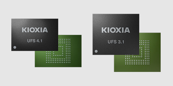
KIOXIA's UFS 4.1/3.1 offers lightning fast embedded storage transfer speeds allowing next-generation smartphones and mobile applications to take advantage of 5G mobile networks.
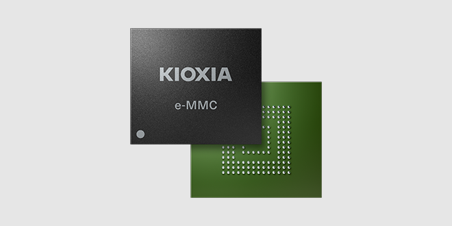
KIOXIA’s lineup of e-MMC products provide an interface compliant with JEDEC Version 5.1, eliminating the need for users to directly control flash memory.
- 1 GB/s is calculated as 1,000,000,000bytes/s, and 1MB/s is calculated as 1,000,000bytes/s. This is a theoretical value calculated from the interface speed and the speed of a user’s device is not guaranteed. The read/write speed may vary depending on the host system, read/write conditions, file size, etc.
- Product density is identified based on the density of memory chip(s) within the Product, not the amount of memory capacity available for data storage by the end user. Consumer-usable capacity will be less due to overhead data areas, formatting, bad blocks, and other constraints, and may also vary based on the host device and application. For details, please refer to applicable product specifications. The definition of 1KB = 2^10 bytes = 1,024 bytes. The definition of 1Gb = 2^30 bits = 1,073,741,824 bits. The definition of 1GB = 2^30 bytes = 1,073,741,824 bytes. 1Tb = 2^40 bits = 1,099,511,627,776 bits.
- Performance figures are based on internal tests. Actual results may vary depending on host device, usage patterns, and other conditions.
- This product supports dual-supply operation at VCC and VCCQ/VCCQ_M. VCCQ2 is not necessary.
- JEDEC is a registered trademark of JEDEC Solid State Technology Association
- MIPI®, M-PHY® and UniPro® are registered trademarks owned by MIPI Alliance.
Support

Please contact us if you have any technical questions, requests for materials, are interested in samples or purchases of business products (Memory, SSD), etc.
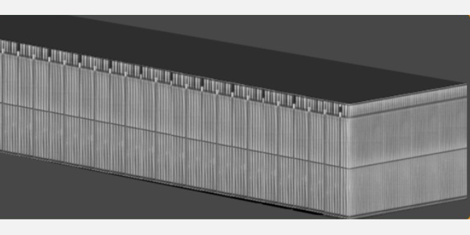
In 2007, KIOXIA announced the world‘s first 3D flash memory technology. Presenting our cutting-edge technologies, along with the key points of innovation and our efforts toward further increases in capacity.
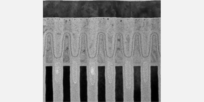
KIOXIA invented the world’s first NAND flash memory in 1987. This is an explanation of the structure of flash memory and the mechanism of data storage.
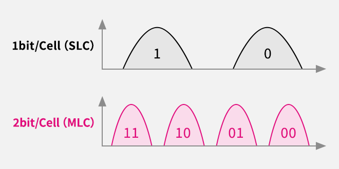
“Multi-level cell technology” is one of the main technologies realizing larger capacity flash memory. The 1 Gbit MLC NAND flash memory launched by KIOXIA in 2001 was the first application in the world of multi-level cell technology to a NAND flash memory product.


