

Please select your location and preferred language where available.
Improved disturb-free memory window, retention and endurance in low-voltage 3D-FeFETs by controlling strain and trap properties in interfacial layers
October 27, 2026
3D-FeFETs with low-operation voltage are promising candidates for low latency and high-density memory by reducing RC delay through reduction of word line length. However, FeFETs still have many challenges, such as read disturbance and endurance, which affect the narrowing of the programable memory window.
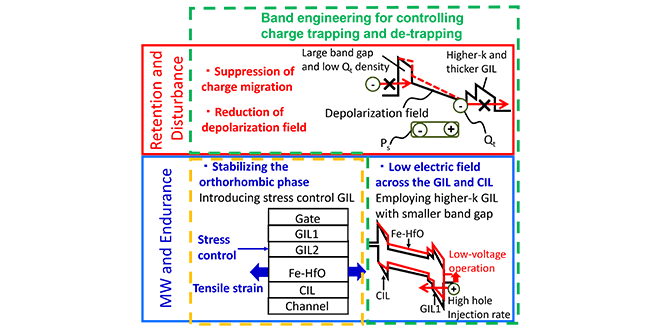
Figure 1 illustrates the FeFET design with a Channel Interfacial Layer (CIL) and stacked Gate Interfacial Layer (GIL) proposed in this study. The polarization (Ps) is enhanced by stabilizing the orthorhombic phase (o-phase) of Ferroelectric HfO (Fe-HfO) through stress control by GIL2, improving MW after endurance. In addition, band engineering utilizing the CIL and stacked GIL to control charge injection and detrapping rates is important for enhancing overall reliability.
©2026 IEEE
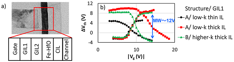
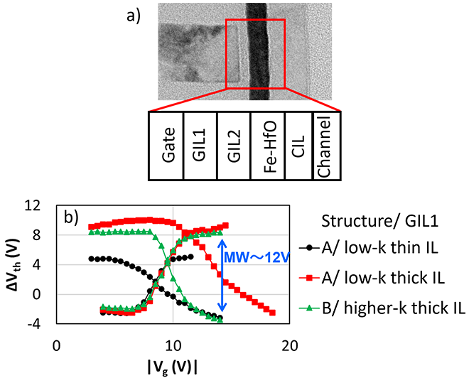
Figure 2(a) shows the cross-sectional TEM image of the 3D-FeFET. A key point is the stacked gate interfacial layer which adjusts the stress of the ferroelectric material and controls charge movement. Figure 2(b) presents the program/ erase characteristics of the 3D-FeFET using gate interfacial layers with different thicknesses and dielectric constants (k). Thicker and higher-k GIL1 enhances the maximum MW and reduces operation voltages, achieving a MW of 12V with an operation voltage below ±14V.
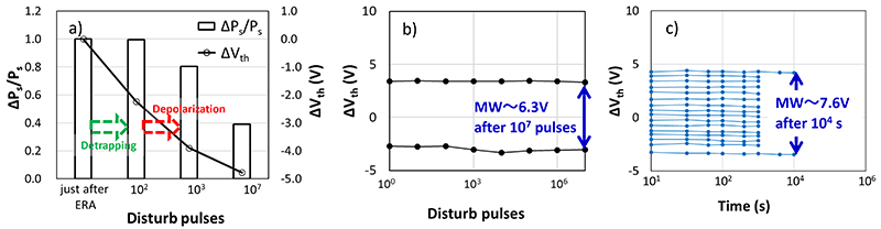
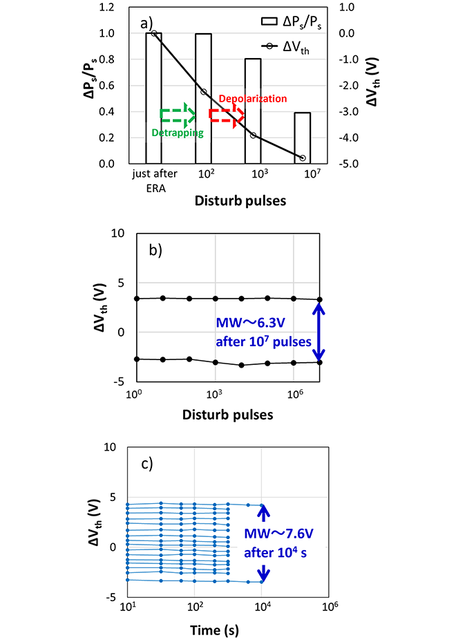
FeFETs have a large programmable memory window; however, not all of the window is accessible for memory operations. This limitation arises because a high Vth state requires a high read-voltage to turn on the unselected cells. Figure 3(a) shows the changes in Vth and remanent polarization ratio (ΔPs/Ps) when 8V read disturb pulses are applied. After applying 102 disturb pulses, only Vth shift can be observed with no changes in polarization. Subsequently, both Vth shifts and polarization reversal occur simultaneously up to 107 pulses. This result indicates that the Vth change due to read disturbance occurs in two steps. In the first step, remanent polarization remains unchanged over 102 cycles, indicating that the detrapping of excessive trapped charge dominates the Vth degradation. In the second step, the electric field across the ferroelectric-HfO increases due to detrapping, leading to depolarization over 107 disturbances. By utilizing a thick and higher-k GIL1 to suppress the movement of the trapped charges, a large memory window can be achieved after read disturbance (see Figure 3(b) and retention (see Figure 3(c)).
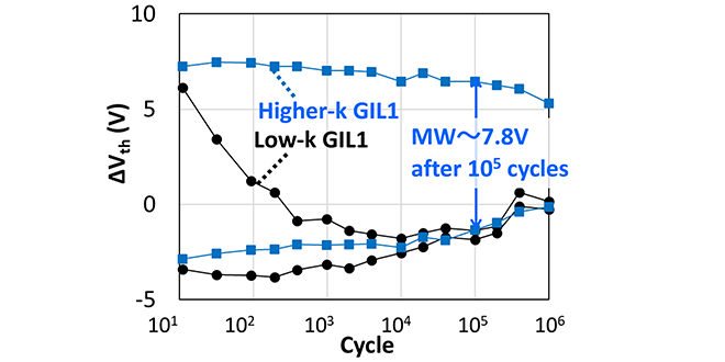
Furthermore, the FeFET with the higher-k GIL1 can reduce the operating voltage compared to the low-k GIL1 by charge injection. As a result, a large memory window after endurance is achieved by suppressing the degradation of the gate and channel side interfacial layer (see Figure 4). Therefore, we consider low-voltage FeFET is a viable candidate for low-latency and high-density storage memory.
This work was presented at VLSI Symposium 2026 (2026 IEEE/JSAP Symposium on VLSI Technology and Circuits) in June 2026.
Reference
[1] K.Suzuki et al., “Improved Disturb-Free Memory Window, Retention and Endurance in Low-Voltage 3D-FeFETs by Controlling Strain and Trap Properties in Interfacial Layers”, 2026 IEEE/JSAP Symposium on VLSI Technology and Circuits, T9-2.

A technical glossary that covers terms related to KIOXIA products and technologies, such as memory and SSDs. We explain that it can be used by engineers and researchers to the general public.

KIOXIA has established industry-leading R&D frameworks with “memory” technology. We use our various locations to conduct technological innovation while promoting open innovation.


