

Please select your location and preferred language where available.
A Multi-Stacked Cell Array Architecture with Wafer-to-Wafer Cu Direct Bonding for Ultra-High-Density 3D Flash Memory beyond 1,000 Word Lines
October 27, 2026
With the rapid growth of data driven by generative AI, 3D flash memory is increasingly required to provide higher capacity and density. One promising approach is to increase the number of stacked word lines. However, as the number of stacked word lines increases, key challenges such as cell current degradation, increased wafer warpage, and larger block size become more severe, making it difficult to realize more than 1,000 stacked word lines.
To address these challenges, a Multi-Stacked cell Array CMOS directly Bonded to Array (MSA-CBA) architecture was developed. As shown in Figure 1, the architecture sequentially stacks two or more memory cell array wafers on a CMOS wafer using wafer-to-wafer Cu direct bonding. By limiting the number of stacked word lines in each array wafer, it structurally mitigates cell current degradation and wafer warpage, even as the total number of stacked word lines increases. In addition, sharing the word line switch circuit among multiple array wafers helps reduce block size and lower power consumption.
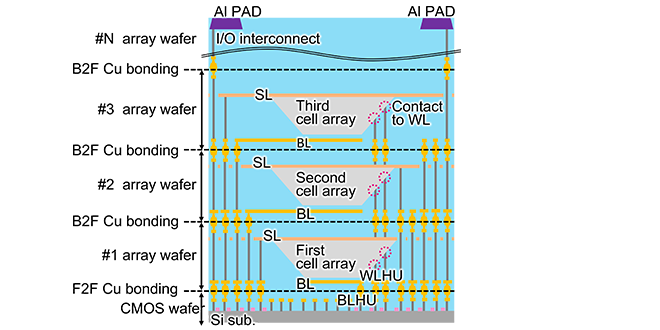
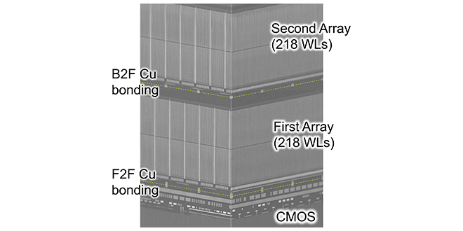
A key enabler of this architecture is a wafer-to-wafer Cu direct bonding process compatible with multi-wafer stacking. To realize reliable multi-wafer integration, technologies were established to planarize the step generated during backside interconnect formation and to correct bonding misalignment between highly warped wafers. As shown in Figure 2, these technologies enabled array wafers with 218 stacked word lines each to be successfully stacked and bonded on a CMOS wafer, demonstrating reliable multi-wafer integration.
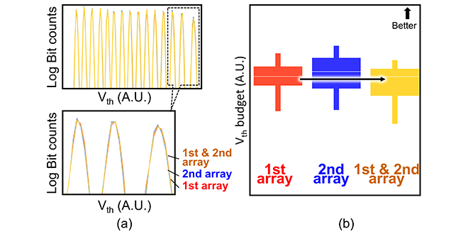
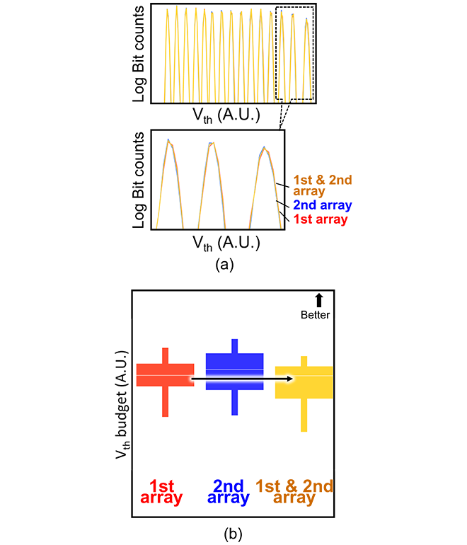
Furthermore, the world’s first Quad-Level Cell (QLC) operation in the MSA-CBA architecture was demonstrated using prototype devices. As shown in Figure 3, the threshold voltage distributions of each programmed state were clearly separated immediately after QLC programming, and sufficient voltage margins were confirmed for both the individual arrays and the overall MSA-CBA structure. Even after a high-temperature data retention test, sufficient margins between threshold voltage distributions were maintained, demonstrating reliable QLC operation in the MSA-CBA architecture.
This technology is an important foundation for realizing next-generation ultra-high-density 3D flash memory with more than 1,000 stacked word lines. This work was presented at VLSI Symposium 2026 (2026 IEEE/JSAP Symposium on VLSI Technology and Circuits) in June 2026.
Reference
[1] Mitsuhiko Noda et al., “A Multi-Stacked Cell Array Architecture with Wafer-to-Wafer Cu Direct Bonding for Ultra-High-Density 3D Flash Memory Beyond 1,000 Word Lines, ” 2026 IEEE/JSAP Symposium on VLSI Technology and Circuits (VLSI Technology and Circuits), T1-4.

A technical glossary that covers terms related to KIOXIA products and technologies, such as memory and SSDs. We explain that it can be used by engineers and researchers to the general public.
KIOXIA has established industry-leading R&D frameworks with “memory” technology. We use our various locations to conduct technological innovation while promoting open innovation.


