

Please select your location and preferred language where available.
Deposition-Process-Based Charge Trap Layer Segmentation for 3D Flash Memory
October 27, 2026
In 3D flash memory, the number of word lines (WLs) has been increased to improve bit density. However, taller memory stacks lead to higher costs and more complicated processes. Therefore, reducing the WL pitch to suppress stack height has attracted attention. On the other hand, WL pitch scaling degrades cell reliability due to cell-to-cell interference and lateral charge loss, in which stored charges migrate toward adjacent cells (Figure 1).
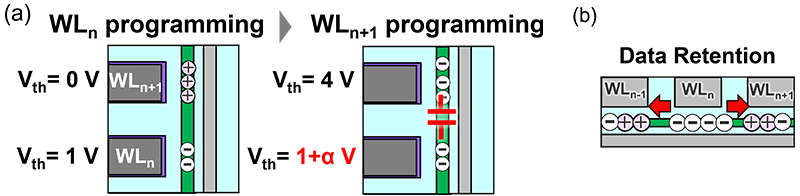
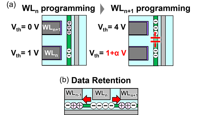
(a) Cell-to-cell interference,(b) Lateral charge loss [1] ©2026 IEEE
To address these issues, we devised a method to reduce the parasitic capacitance between adjacent cells and the charge migration path by segmenting the Charge Trap Layer (CTL). If the CTL between adjacent WLs is completely removed, programming efficiency is significantly degraded [1][2]. Therefore, we adopted a Pseudo-segmented CTL that reduces the thickness of the CTL connecting adjacent cells while maintaining both improved cell reliability and programming efficiency. Figure 2(a) shows the proposed fabrication flow. After removing the sacrificial film and spacer layer, an Area Selective Deposition (ASD) process is introduced to selectively deposit silicon nitride (SiN) only on the seed SiN layer. This enables the formation of a Pseudo-segmented CTL structure. In addition, this process can prevent an increase in memory hole diameter by adjusting the thickness of the spacer layer. Figure 2(b) shows cross-sectional images of the fabricated prototype device with more than 100 WLs. We confirmed that the Pseudo-segmented CTL structure can be formed through a deposition-process-based approach utilizing ASD technology.
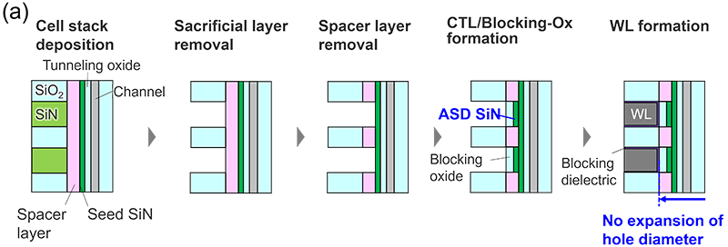
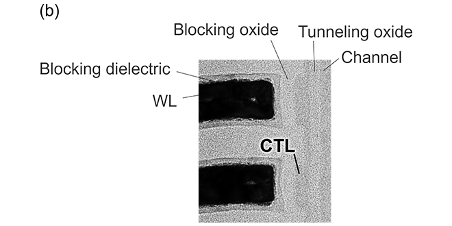
(a) Fabrication Flow,(b) Cross-Sectional TEM Image of the Prototype Memory Cell [1] ©2026 IEEE
Figures 3 and 4 show the cell array characteristics of the prototype. In the threshold voltage (Vth) distribution after Triple Level Cell (TLC) programming, the Pseudo-segmented CTL suppressed the distribution broadening caused by cell-to-cell interference by 29%. In addition, the data retention characteristics showed a 44% reduction in lateral charge loss. As a result, the widening of the Vth distribution during high-temperature data retention was significantly suppressed in the TLC distribution before program/erase stress.
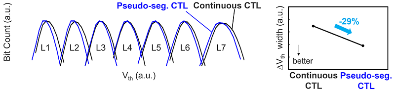
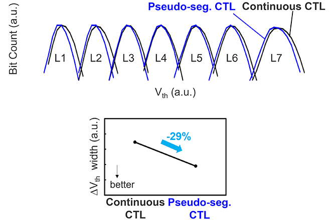
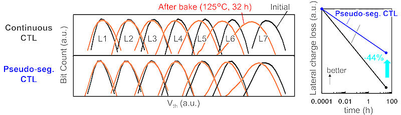
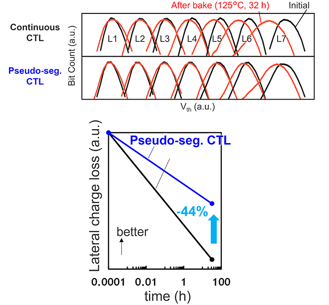
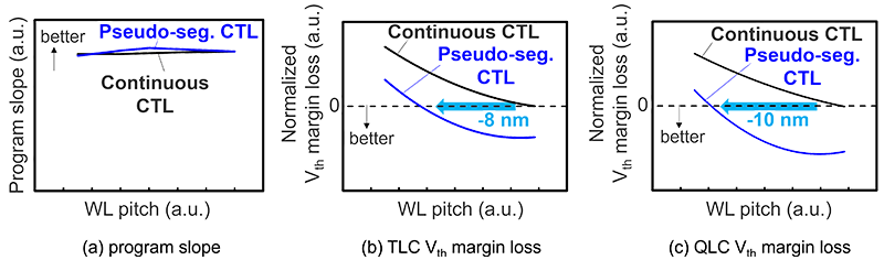
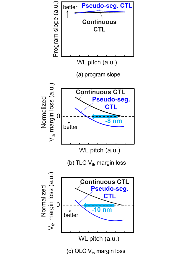
Figure 5 shows the WL pitch scalability from a cell reliability perspective, as predicted by Technology Computer-Aided Design (TCAD) simulation. Cell reliability is evaluated using the threshold voltage (Vth) margin before program/erase stress. The Pseudo-segmented CTL is estimated to enable WL pitch scaling down to 8 nm for TLC and 10 nm for Quadruple Level Cell (QLC), while maintaining programming efficiency comparable to that of continuous CTL cells. Thus, Pseudo-segmented CTL has strong potential to advance WL pitch scaling in 3D flash memory.
This work was presented at VLSI Symposium 2026 (2026 IEEE/JSAP Symposium on VLSI Technology and Circuits) in June 2026.
Reference
[1] F. Kikushima et al., “Deposition Process-Based Charge Trap Layer Segmentation for 3D Flash Memory Achieving Improved Cell Reliability While Maintaining Program/Erase Characteristics”, 2026 IEEE Symposium on VLSI Technology and Circuits, Jun. 2026, pp. 1-4.
[2] S.-W. Jin et al., “A Highly Scalable Isolated Charge Trap Nitride Layer Implemented in a 176-layer 3D NAND Flash with Superior Threshold Voltage Distribution and Charge Retention”, IEEE International Electron Devices Meeting (IEDM), Dec. 2025, pp. 1-4.

A technical glossary that covers terms related to KIOXIA products and technologies, such as memory and SSDs. We explain that it can be used by engineers and researchers to the general public.
KIOXIA has established industry-leading R&D frameworks with “memory” technology. We use our various locations to conduct technological innovation while promoting open innovation.


