

Please select your location and preferred language where available.
Ultra-thin Mo/Poly-Si Stacked Hybrid Floating Gate for Enhanced Program Efficiency in 3D Flash Memory
September 28, 2026
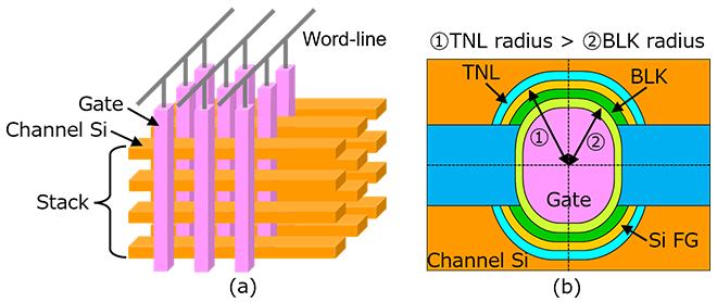
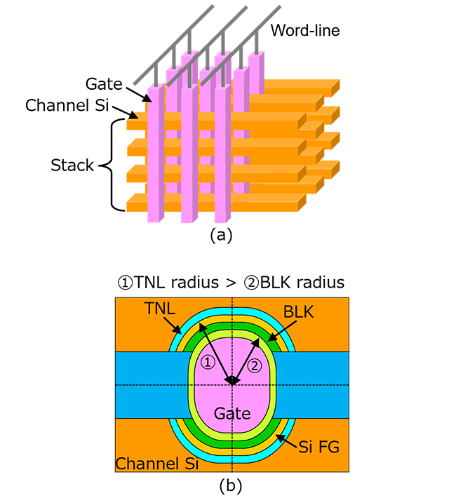
3D flash memory has achieved high bit density with low cost by increasing the number of cell stacked cell layers[1]. The cell current decreases as the number of stacks increases, which is a serious issue. As an alternative, a new architecture called Horizontal Channel Flash (HCF) in Figure 1(a) has been proposed due to the independence of cell current from the number of stacked layers[2]. In the HCF cell, as shown in Figure 1(b), the radius of the tunnel oxide (TNL) is larger than that of the blocking oxide (BLK), indicating an inverse curvature effect that makes it difficult to establish a stronger electric field in the TNL compared to the BLK, thereby hindering the achievement of an adequate program characteristic.
We have proposed an HCF cell structure with a metal/Si Hybrid Floating Gate (HFG), in which an ultra-thin metal film is inserted between the Si Floating Gate (Si FG) and the BLK, as shown in Figure 2(a) [3]. As shown in the energy band diagram in Figure 2(b), most ballistic electrons passing through the TNL are trapped by the metal in the HFG, thereby reducing the number of electrons penetrating the BLK. Theoretically, it is possible to enhance the program characteristics.
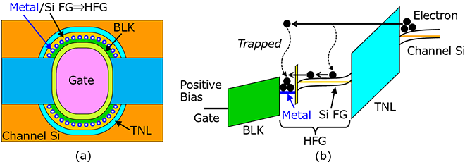
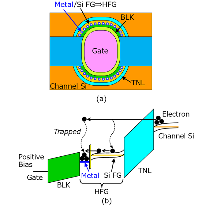
Figure 3(a) compares the program characteristics evaluated using planar cell capacitors of Mo/Si HFG, TiN/Si HFG, and Si FG cells, each of which features ultra-thin Mo and TiN films, respectively. The results reveal that the program efficiency is enhanced in the HFG cells with the ultra-thin metal layer (0.1nm). Furthermore, the program slope of the metal/Si HFG cells achieves the ideal value of 1 V/V in Figure 3(b). On the other hand, the superior improvement achieved with Mo compared with TiN indicates that the high thermal stability of Mo prevents BLK degradation caused by metal diffusion.
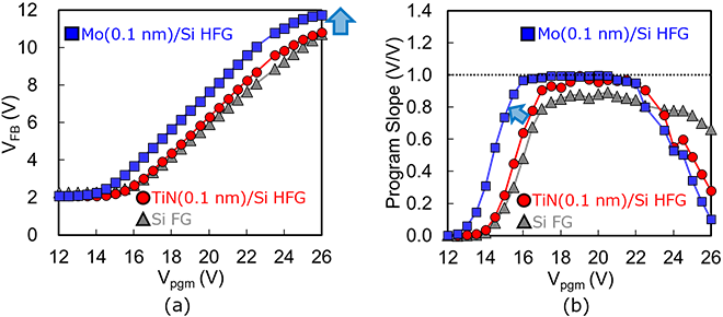
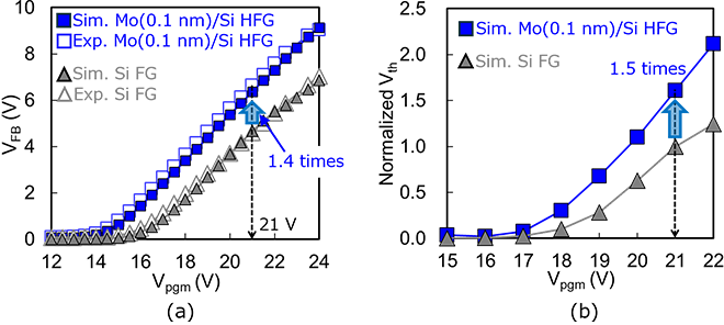
Figure 4(a) compares the experimental program characteristics, normalized by the neutral VFB values, with those simulated by Technology Computer-Aided Design (TCAD) for the planar Mo/Si HFG and Si FG cells. The simulated results are in good agreement with the experimental characteristics, and the VFB value of the Mo (0.1nm)/Si HFG cell at Vpgm of 21V is approximately 1.4times larger than that of the Si FG cell. Figure 4(b) shows the program characteristics simulated by TCAD for the cells illustrated in Figure 2(a), using the planar cell simulations. The normalized threshold voltage (Vth) of the Mo (0.1nm)/Si HFG cell at Vpgm of 21V is more than 1.5times larger than that of the Si FG cell, demonstrating an enhancement in efficiency for the cells exhibiting the inverse curvature effect.
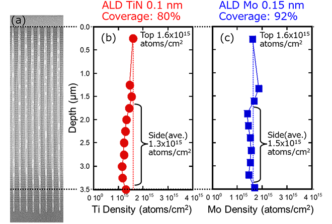
It is essential to control the sub-nanometer range thickness, while ensuring conformal coverage from the top to the bottom of the high aspect ratio Memory Holes (MH). Figure 5(b) and Figure 5(c) show the depth profiles of the areal densities of Ti and Mo, respectively, in the MH structure shown in the cross-sectional Transmission Electron Microscopy (TEM) image in Figure 5(a). The areal densities were evaluated using Laser Ablation Inductively Coupled Plasma Mass Spectrometry (LA-ICP-MS) analysis. Ultra-thin TiN and Mo films were deposited by Atomic Layer Deposition (ALD) using TiCl4 and MoO2Cl2 as the respective precursors. At a thickness of 0.15nm, Mo achieves a side/top coverage ratio of 92%, indicating superior coverage compared to TiN.
These findings confirm that the combination of HCF and Mo-based HFG represents a promising candidate for future 3D flash memory.
This achievement was presented at the IEEE IMW 2026(IEEE International Memory Workshop 2026).
Reference
[1] H. Tanaka et al., “Bit Cost Scalable Technology with Punch and Plug Process for Ultra High Density Flash Memory”, in Proc. 2007 IEEE Symposium on VLSI Technology and Circuits
[2] M. Oda et al., “Superior Scalability of Advanced Horizontal Channel Flash for Future Generations of 3D Flash Memory”, in Proc. 2024 IEEE International Electron Devices Meeting (IEDM)
[3] D. Ikeno et al., “Ultra-thin Molybdenum/Polysilicon Stacked Hybrid Floating Gate for Enhanced Program/Erase Efficiency in 3D Flash Memory”, in Proc. 2026 IEEE International Memory Workshop (IMW)

A technical glossary that covers terms related to KIOXIA products and technologies, such as memory and SSDs. We explain that it can be used by engineers and researchers to the general public.

KIOXIA has established industry-leading R&D frameworks with “memory” technology. We use our various locations to conduct technological innovation while promoting open innovation.


