

Please select your location and preferred language where available.
Development of a 10th Generation 2Tb 4b/cell BiCS FLASH™ product
July 15, 2026
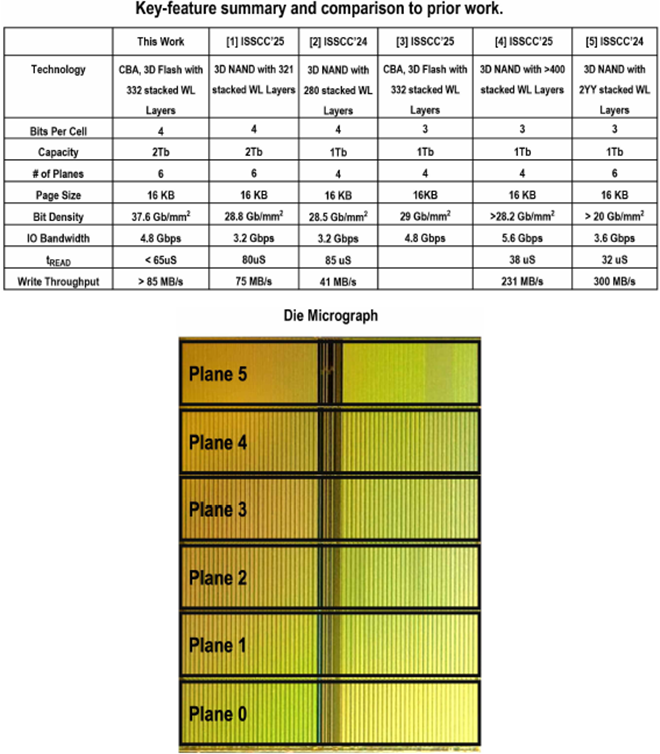
Preceding the 3bit/cell(TLC) presentation from last year, we presented the development of a 10th generation BiCS FLASH™ 2Tb 4b/cell product at the international conference ISSCC2026. [1]
This product is developed by Kioxia and Sandisk Corporation and it consists of features such as, a 332 stacked word-line[2], and high-density floor plan technique.
A bit density of 37.6Gb/mm2 was achieved for this chip, the highest bit density amongst QLC products (Figure 1).
We also achieved over 85MB/s of high write throughput by introducing performance improvement technique including new sensing technique, “Local BUS(LBUS) Coupling Sense” (Figure 1).
In addition to this, we also developed a new power reduction technique, “Bus Idle Sleep” for super multi-stacked package needed for matured AI development.
High-density floor plan, LBUS Coupling Sense, and Bus Idle Sleep, the 3 key highlights of this product are briefly explained below.
High-density floor plan technique
This product adopts the CBA (CMOS directly Bonded to Array) structure[3], consistent with previous products, and implements a 6-plane architecture for the first time in our QLC products.
By employing a 1×6 floorplan instead of the 2×3 configuration, it reduces the bonding pad (BP) area, thereby achieving a reduction in the overall die area (Figure 2).
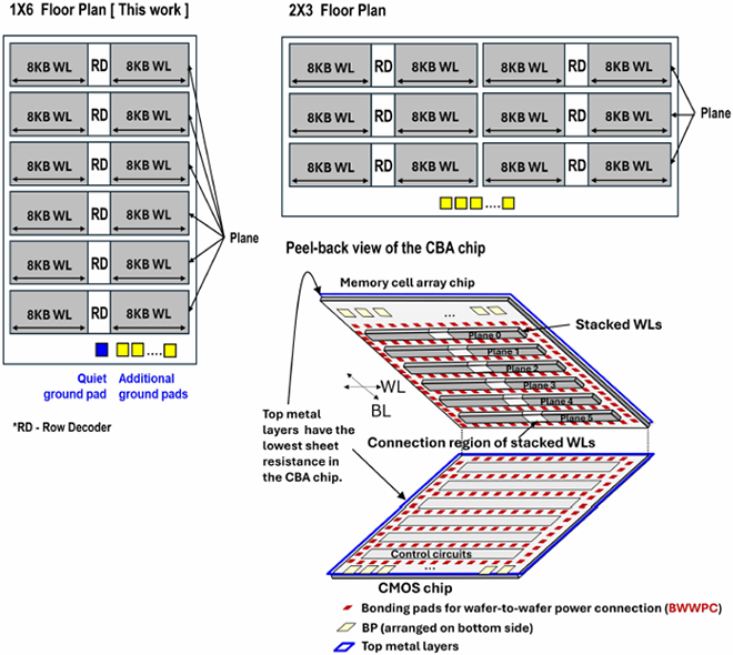
To achieve a 1x6 floor plan, the following challenges were addressed:
- Increased vertical power supply resistance due to the reduction of the BP region.
- Ground bounce resulting from the increased vertical length of the chip.
- Increased inter-plane asynchronous read noise due to the 6-plane structure.
To address the first challenge, the flexibility of CBA process modifications was leveraged to introduce a dedicated metal wiring layer for power distribution enhancement, thereby mitigating the resistance increase.
Regarding the second challenge, pad placement was optimized, and the number of ground pads was expanded, reducing the ground bounce to an acceptable level.
Furthermore, to address the third challenge, dedicated quiet ground pads were added for noise-sensitive circuits. Through these countermeasures, a world-record density of 37.6 Gb/mm² was achieved while minimizing the impact on circuit operation.
LBUS Coupling Sense
Write throughput degradation is a critical challenge in QLC products due to the increased number of states to be written compared to TLC products.
To mitigate this issue, a novel high-speed sensing technique has been introduced.
By exploiting the coupling between SEN2 and LBUS in the conventional Local CLK circuit[3] shown in the circuit schematic in Figure 3, the sense results of SEN2 are read directly to LBUS without passing through the SEN node.
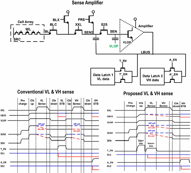
In general, in verify operation, which checks whether each state has reached the target write level, sensing is performed twice at VL (slightly below the target write level) and VH (the target write level) to achieve a sharper write distribution.
In conventional technique, both VL and VH sense results are latched into Data Latch 1 and 2 via the SEN.
Consequently, a setup operation for VH sensing is required after the VL sensing is completed, as shown in the left timing diagram in Figure 3.
In contrast, the proposed technique utilizes the other path.
Here, the VL sense result is transferred directly to Data Latch 1 via the LBUS coupled by SEN2, rather than via the SEN.
This configuration leaves the SEN unaffected, allowing the setup operation required in the conventional technique to be omitted.
As a result, VH sensing can be executed in parallel, achieving a 4.2% improvement in write throughput, as illustrated in the right timing chart in Figure 3.
Bus Idle Sleep
Driven by the recent proliferation of AI applications, the demand for higher-density storage has increased, and the development of super multi-stacked package is key to realizing this demand.
However, as illustrated in Figure 4, non-selected chips within the package remain idle, awaiting high-speed Data Input/Output operations, thereby generating standby (bus idle) current.
Moreover, the recent increase in stack height has led to a greater number of non-selected chips, causing the idle current consumed by these chips to become non-negligible.
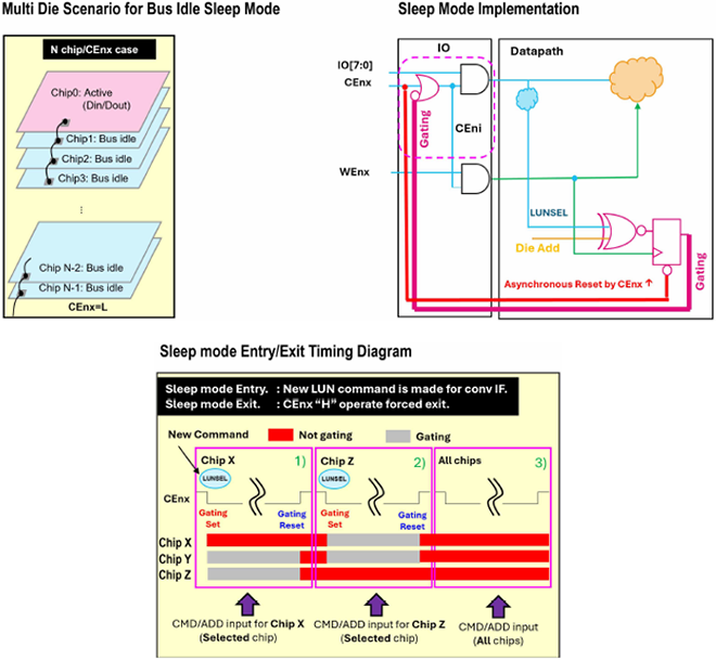
To mitigate this current, a new technique has been implemented to reduce the idle current of non-selected chips to levels comparable to standby current prior to large number of non-selected chips.
Conventionally, activating the CE (Chip Enable) pin resulted in idle currents on the order of 10’s of mA, even in non-selected chips.
In the proposed technique, as illustrated in the circuit schematic in Figure 4, non-selected chips are automatically forced into an internal standby state via a gating signal (indicated in pink) that signifies non-selection, regardless of the activation of the external CE pin.
Consequently, the current consumption is reduced to the order of 100’s of µA.
As we have introduced so far, high density floor plan and performance/power improvement techniques are effective technologies for the continuous improvement of memory density, cost reduction and performance improvement in 3D flash memory.
We will continue to advance these technologies and integrate them into our future products, delivering greater value and more compelling solutions to our customers.
This achievement was presented at the ISSCC2026.
Reference
[1] J. M. Thimmaiah et al., "A 2Tb 4b/Cell 6-Plane 3D-Flash Memory with 37.6Gb/mm2 Bit Density and >85MB/s Write Throughput," 2026 IEEE International Solid-State Circuits Conference (ISSCC), San Francisco, CA, USA, 2026, pp. 254-256, doi: 10.1109/ISSCC49663.2026.11409136.
[2] K. Yanagidaira et al., “30.2 A 1Tb 3b/cell 3D Flash Memory with a 29%-Improved-Energy-Efficiency Read Operation and 4.8Gb/s Power-Isolated Low-Tapped-Termination I/Os,” ISSCC, pp506-507, 2025. © 2025 IEEE
[3] H.Maejima et al., “Crossed Bit Line (CBL) Architecture in 3D Flash Memory CMOS Directly Bonded to Array (CBA) Structure”, IEEE International Memory Workshop (IMW), pp.25-28, May.2025.

A technical glossary that covers terms related to KIOXIA products and technologies, such as memory and SSDs. We explain that it can be used by engineers and researchers to the general public.
KIOXIA has established industry-leading R&D frameworks with “memory” technology. We use our various locations to conduct technological innovation while promoting open innovation.


