Please select your location and preferred language where available.
Spin-orbit torque driven motion of chiral domain walls induced by radial magnetization in nanotube geometry
December 23, 2025
We are developing magnetic domain wall memory, which records information by creating an arrangement of magnetized regions within a magnetic nanowire medium. The boundary between areas where the magnetization direction is aligned (magnetic domains) is referred to as a “domain wall” where the magnetization configuration twists (see Figure 1(a)). When current is passed through the nanowire, the spin angular momentum of the conduction electrons affects the domain wall, causing it to shift its position. This phenomenon is the basis of magnetic shift registers, which are expected to serve as next-generation high-capacity storage solutions.
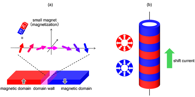
To achieve terabit-level storage, our research focuses on developing the three-dimensional (3D) nanotube structure shown in Figure 1(b)[1]. We aim to induce a radial magnetization direction within the nanotube structure by using perpendicular magnetic anisotropy (PMA) materials in the magnetic domain wall motion layer. This approach could enable the use of spin orbit torque (SOT)[2], which can shift magnetic domain walls more efficiently than the conventional spin transfer torque (STT), promising low power consumption.
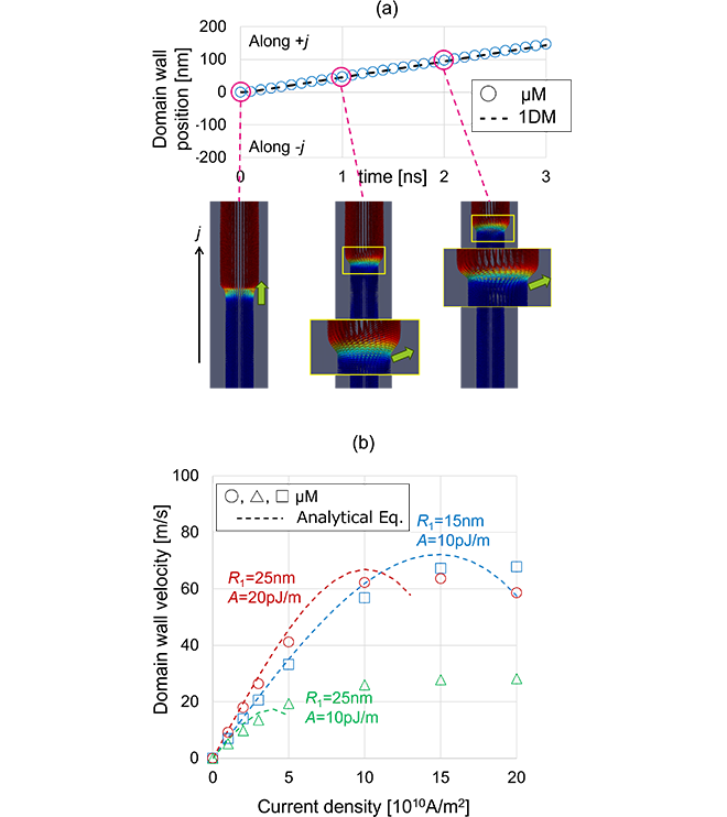
Since prototyping and evaluation of 3D magnetic domain wall devices require advanced technology, there are no experimental reports on current-driven domain wall motion in nanotube structures at present. For this demonstration, it is crucial to elucidate the geometrical effects associated with the 3D structure through theoretical studies and to provide feedback on these insights into the design of the domain wall motion layer. In this study, we formulated the phenomenon of SOT-driven domain wall motion using a one-dimensional model (1DM)[3]. We also validated this model using high precision micromagnetic (µM) simulations[3], which is a TCAD method. As a result, we clarified the mechanism of SOT-driven domain wall motion in PMA nanotubes and enabled the rapid quantitative prediction of shift characteristics.
To incorporate the geometrical effects of PMA nanotubes into 1DM, we derived expressions for effective magnetic fields acting on domain walls inside the nanotubes. One example of the effective magnetic field specific to PMA nanotubes is the stray field arising from the magnetic domain regions, shown in Figure 2(a). As shown in Figure 2(b), this effective magnetic field increases as the nanotube diameter decreases and induces a chiral Néel domain wall state. Since the efficiency of SOT-driven motion increases as the domain wall is more strongly fixed in the Néel state, the domain wall motion speed in PMA nanotubes is generally higher than in 2D flat magnetic nanowires made of the same material.
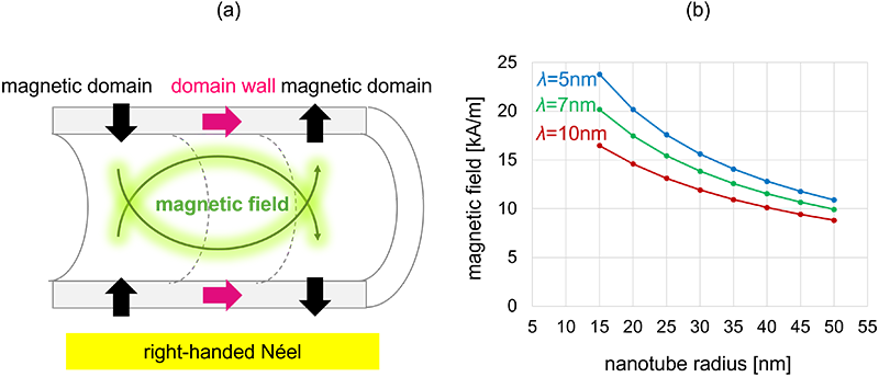
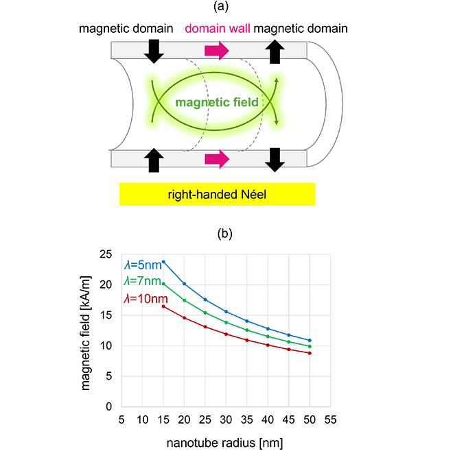
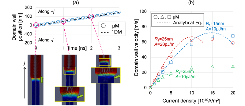
Figure 3(a) shows an example of the simulation results of domain wall motion in a PMA nanotube. Using μM simulations and a 1DM model independently, we demonstrated for the first time that domain walls can be driven by SOT to move along a nanotube[4]. Figure 3(b) shows the domain wall velocity as a function of current density. It shows that domain wall velocity depends not only on current density but also on the nanotube diameter and magnetic properties such as the exchange stiffness constant. We revealed that PMA nanotubes have specific knobs for controlling shift characteristics and provided important insights for device design.
This achievement was published in the academic journal "Physical Review B" on September 11, 2025 (Phys. Rev. B 112 , 094425, DOI: https://doi.org/10.1103/ngkw-t9r8![]() )。
)。
Reference
[1] M. Quinsat et al., Demonstration of Reliable Magnetic Shift Register Reading Using 50 nm MTJs on CMOS IC Towards 3D Ultra-High Density Memory, EDTM 2025.
[2] N. Umetsu et al., J. Magn. Magn. Mater. 614, 172738 (2024).
[3] E. Martinez et al., J. Appl. Phys. 116, 023909 (2014).
[4] N. Umetsu et al., Theoretical study of current induced domain wall motion in perpendicularly magnetized nanotubes in three-dimensional magnetic shift register, Joint MMM-Intermag 2025.
[5] N. Umetsu et al., Phys. Rev. B 112, 094425 (2025).

A technical glossary that covers terms related to KIOXIA products and technologies, such as memory and SSDs. We explain that it can be used by engineers and researchers to the general public.

KIOXIA has established industry-leading R&D frameworks with “memory” technology. We use our various locations to conduct technological innovation while promoting open innovation.