Please select your location and preferred language where available.
Toshiba Launches Industry's Largest[1] Embedded NAND Flash Memory Modules
e •MMCTM[2] Compliant Embedded Memories Combine up to 128GB NAND and a Controller in a Single Package
- June 17, 2010
TOKYO—Toshiba Corporation (TOKYO: 6502) today announced the launch of a 128-gigabyte (GB) embedded NAND flash memory module, the highest capacity yet achieved in the industry. The module is fully compliant with the latest e •MMCTM standard, and is designed for application in a wide range of digital consumer products, including smartphones, tablet PCs and digital video cameras. Samples will be available from September, and mass production will start in the fourth quarter (October to December) of 2010.
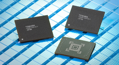
The new 128GB embedded device integrates sixteen 64Gbit (equal to 8GB) NAND chips fabricated with Toshiba's cutting-edge 32nm process technology and a dedicated controller into a small package only 17 x 22 x 1.4mm[3]. Toshiba is the first company to succeed in combining sixteen 64Gbit NAND chips, and applied advanced chip thinning and layering technologies to realize individual chips that are only 30 micrometers thick.
Toshiba now offers a comprehensive line-up of single-package embedded NAND Flash memories in densities from 2GB to 128GB. They integrate a controller to manage basic control functions for NAND applications, and are compatible with the JEDEC e •MMCTM Version 4.4 and its features. New samples of 64GB chips will also be available from August.
Demand continues to grow for large density chips that support high resolution video and deliver enhanced storage, particularly in the area of embedded memories with a controller function that minimizes development requirements and eases integration into system designs. Toshiba has established itself as an innovator in this key area, and is now reinforcing its leadership by being first to market with a 128GB generation module.
New Product Line-up
Product Number |
Capacity |
Package |
Sample Shipment |
Mass Production |
|---|---|---|---|---|
THGBM2T0DBFBAIF |
128GB |
237Ball FBGA |
Sep. 2010 |
4Q, 2010 (Oct.-Dec.) |
THGBM2G9D8FBAIF |
64GB |
237Ball FBGA |
Aug. 2010 |
4Q, 2010 |
Key Features
- The JEDEC e •MMCTM V4.4 compliant interface handles essential functions, including writing block management, error correction and driver software. It simplifies system development, allowing manufacturers to minimize development costs and speed up time to market for new and upgraded products.
- Embedded in a system, the module can record up to 2,222 hours of music at a 128Kbps bit rate, 16.6 hours of full spec high definition video and 38.4 hours of standard definition video[4].
- The 128GB device stacks sixteen 64Gbit chips fabricated with leading-edge 32nm process technology. Application of advanced chip thinning, layering and wire bonding technologies has allowed Toshiba to achieve individual chips only 30 micrometers thick, and to layer and bond them in a small package. The result is an embedded NAND flash memory module with the industry's highest density.
- The new products are sealed in a small FBGA package only 17 x 22 x 1.4mm and has a signal layout compliant with the JEDEC e•MMCTM V4.4.
Specifications
e •MMCTM
Interface |
JEDEC e •MMC TM V4.4 standard HS-MMC interface |
|---|---|
Power Supply Voltage |
2.7V to 3.6V (memory core); |
Bus width |
x1, x4, x8 |
Write Speed * |
21MB per sec. (Sequential/ SDR Mode) |
Read Speed * |
46MB per sec. (Sequential/ SDR Mode) |
Temperature range |
-25degrees to +85degees Celsius |
Package |
153Ball FBGA (+84 support balls) |
* Target figures.
Notes:
[1] For embedded NAND flash memory modules. Source: Toshiba, June 2010.
[2] e •MMC TM is a trademark and a product category for a class of embedded memory products built to the JEDEC e •MMC TM Standard specification.
[3] Planned to be standardized to JEDEC specification
[4] HD and SD are calculated at average bit rates of 17Mbps and 7Mbps, respectively.