Please select your location and preferred language where available.
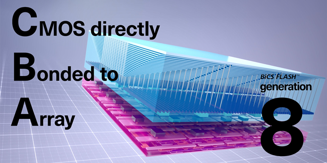
Leading the AI Evolution with Innovative 2mm Flash Memory Assembly Technology
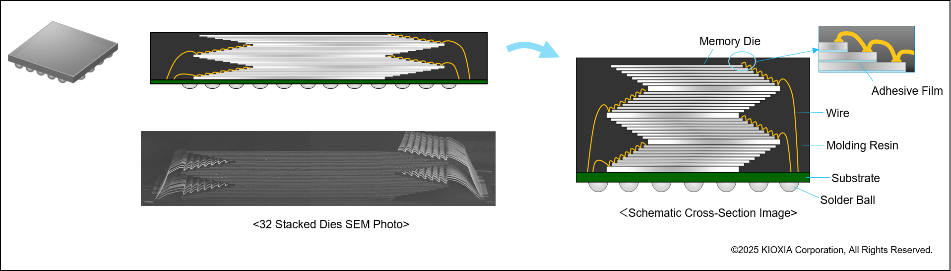
32 memory dies assembled into a single package
Reprinted from: EE Times.com / EE Times.eu
Reprinted from content published in EE Times.com / EE Times.eu on September 26, 2025
This content is used with permission from EE Times Japan.
Department names and titles are as of the time of the interview.
The rapid growth of AI has accelerated demand for flash memory capacity. KIOXIA has successfully developed large-capacity 8 TB (terabyte) flash memory by assembling 32 pieces of 2 Tb (terabit) memory dies into a package less than 2 mm in height. This achievement was made possible with advanced assembly process technologies, including the technology for making wafers as thin as possible.
With the expansion of AI, storing data is more important than ever
With the rapid expansion of AI services, the volume of data handled by data centers has increased exponentially. In addition to the explosive growth of generative AI in recent years, the increased use of retrieval-augmented generation (RAG), which is designed to eliminate the risk of AI hallucinations, further accelerates data growth. In this context, SSDs used in data centers and the flash memory that makes up the SSDs, have become indispensable.
“Following the exponential increase in data volume, the demand for higher-performance and larger-capacity SSDs has accelerated,” says Chiaki Takubo, Technology Executive, Package and Test Technology at KIOXIA Corporation. Moreover, the need for lower power consumption and lower costs has also increased. KIOXIA has anticipated these trends and planned performance and capacity improvements of both SSDs and the underlying flash memory.
Working to increase performance and capacity, KIOXIA has developed 2 Tb (terabit) QLC (Quad-Level Cell) BiCS FLASH generation 8*1 3D flash memory in 2024 as its latest innovation to the 3D flash memory industry. This product introduced the CMOS Directly Bonded to Array (CBA) architecture, where the CMOS circuitry that controls memory cells and the memory cell array are fabricated on separate wafers, which are then bonded together. By stacking 16 memory dies of the BiCS FLASH generation 8 in a single package, it is now possible to achieve a capacity of 32 Tb (terabits), or 4 TB (terabytes) *2.
8 TB capacity made possible by advanced assembly process technology for memory
While CBA is a wafer manufacturing processing technology for semiconductors that is directly responsible for increasing flash memory performance, the evolution of wafer manufacturing processing must be accompanied by the evolution of assembly processes for flash memory as well. Such assembly processing involves stacking memory dies and assembling them in packages.

Increases in flash memory capacity are driven by two factors: increased capacity per die, which is achieved by improving the wafer manufacturing processes, and increased capacity per package, which is achieved by improving the assembly processes. To meet the demand for higher-capacity flash memory, progress must be achieved in both wafer manufacturing, as well as assembly processing. Moreover, it has become particularly important to accelerate the evolution of assembly processes, since wafer manufacturing processes have grown more complex in recent years.
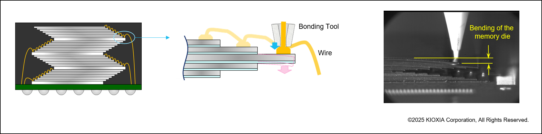
By developing advanced assembly technology, KIOXIA has succeeded in stacking 32 pieces of 2 Tb memory dies into a single package less than 2 mm height (JEDEC standard size: 11.5 x 13.5 mm). By achieving the milestone of placing 8 TB on a single flash memory unit, KIOXIA has taken another major step forward increasing the capacity of SSDs. “We’ve packed all of KIOXIA’s assembly process technology and know-how into this product,” says Takubo. “More specifically, we were able to achieve such a high capacity utilizing three distinct technologies: high-accuracy wafer processing, material design, and wire bonding.”
Innovative assembly technology for stacking 32 dies in a package just 2 mm in height
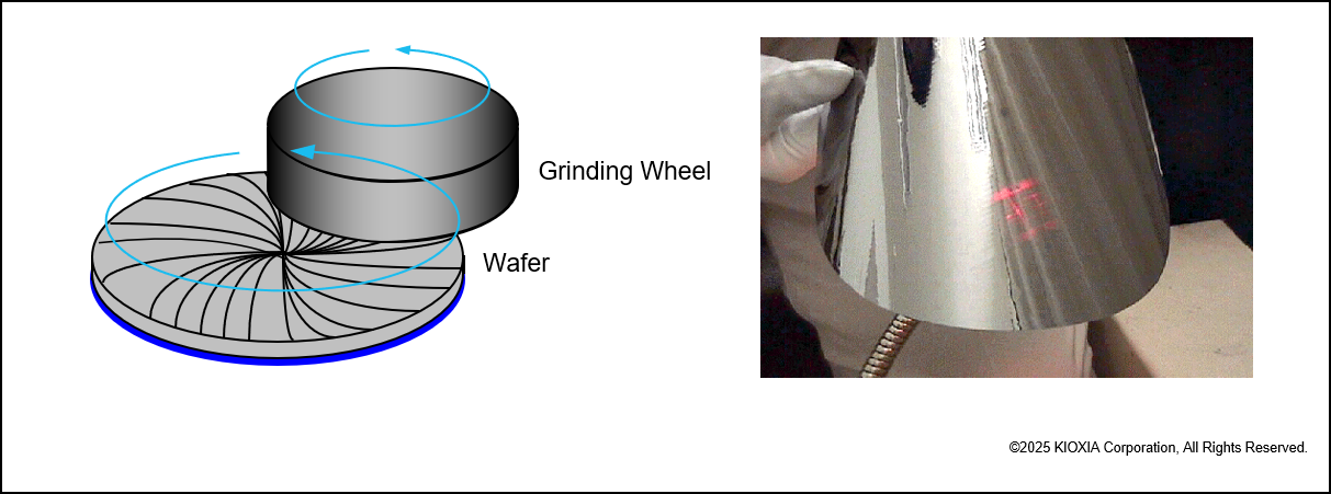
The first technology involved is high-accuracy wafer processing. It is the key to produce memory dies as thin as possible in order to increase the number of dies that can be stacked in a package. This technology contributes to a direct increase in memory capacity per package.
At KIOXIA, 300mm wafers are ground from a thickness of 0.8 mm to 30–40 μm. As a result of this process, thickness is controlled to a thickness accuracy of 0.1 μm. This is equivalent to grinding a massive piece of ice the size of a skating rink (60 x 30 m) to a thickness of 5 mm, with a uniform grinding tolerance of 0.5 mm. This analogy gives you an idea of the advanced precision of the grinding process.
If a single die increases in thickness by 2 μm, stacking 32 layers would result in a total thickness of 64 μm. This would expose the dies and wire-bonding wires outside of the package, making it impossible to ensure quality. Wafers are processed to be as thin as possible to maximize the number of die layers, while ensuring quality at the same time.
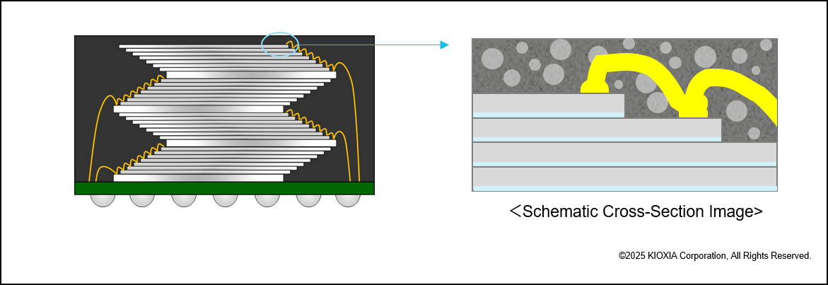
The second technology involved is material design, which is the need to create the molding resin used in the package. In assembly processing, dies are stacked and wires are bonded to the lower substrate to make the electrical connection. The molding resin is then poured into a mold to seal and complete the package. The key point here is the thickness between the topmost stacked dies and wires, and the top of the package (resin thickness above the dies). If the thickness is insufficient, the dies and wires will show through or the wires will be exposed. Since this would negatively affect quality and reliability testing, the molding resin on the die must be formed to a precise thickness of 100 μm. This requires a molding resin with optimal physical properties in terms of flow and filling. Because developing such a molding resin is not an easy task, KIOXIA works closely with material manufacturers to design the precise materials.
The third critical technology is wire bonding. Dies are stacked in layers and shifted sideways at increments for the wire bonding process. A portion of the die overhang like eaves, and inevitably bend during wire bonding. For this reason, specific stress and control conditions for wire bonding are required to prevent the die from cracking due to excessive force. KIOXIA continually develops specifications to meet all of these requirements and then incorporates them into the manufacturing process. “For wire bonding, we control the load gradually to prevent cracks from occurring. Extremely fine adjustments are made within a very short bonding time. The technology used to create such conditions is also one of KIOXIA’s strengths and is critical to our advanced assembly technology,” says Takubo.
Assembly processing designed to optimize and integrate all materials and tools
Even considering just the three technologies above, it is easy to see that the assembly techniques used are extremely sophisticated. However, many other technology elements have also been optimized for KIOXIA’s assembly processing. These elements include the adhesive film used when stacking dies, and the package substrate design, to ensure high signal integrity, power integrity, and reliability. Additionally, increasing the number of dies stacked causes the problems of die warpage and difficulty focusing the lens of the wire bonding machines, due to the large difference in height between the topmost and bottom dies. In order to resolve these issues, all materials and tools are individually optimized. By repeating these intricate and continual optimizations and integrating them into the assembly processes, KIOXIA has made high-capacity flash memory possible.
Furthermore, in order to meet the ever growing demand for greater capacity, KIOXIA is developing next-generation packaging technology. “KIOXIA has a profound knowledge of materials and equipment, and its strength lies in the open and active discussions between all departments responsible for the wafer manufacturing process and assembly processes of flash memory and SSD development. For example, we are constantly collaborating on development of structures to increase the number of stacked dies in a single package, such as structures that fit stacked dies together like twin towers,” says Takubo.
Enabling progress of AI through advanced back-end processing
According to Takubo, “If we make a comparison with the human body, semiconductors, such as CPUs, are equivalent to important parts like the brain, heart, and internal organs. The equivalent of blood vessels and muscles connecting these semiconductors and electronic components is the packaging technology, which is the assembly processes. With the blood vessels and muscles, all organs function organically, and the body as a whole can optimize and maximize its functions—this is the essence of packaging technology. I think we are now at a point in time where it is difficult to improve performance unless we strengthen assembly process technology.”
The number of stacked dies in a package for KIOXIA’s flash memory has doubled from 16 to 32 in just one year. The basic technology for 32 die stacking had first been considered about eight years ago, but since market demand was still insufficient, it was not commercialized,” says Takubo. However, the situation is very different today. As the AI megatrend continues, there will be strong demand for larger flash memory capacities in the foreseeable future. “KIOXIA’s role is to quickly deliver flash memory and SSDs to customers that possess the following qualities: high capacity, high speed, small size, and low power consumption,” emphasizes Takubo. KIOXIA is determined to innovate in the ever evolving AI era, which is expected to accelerate in the future, not only through wafer manufacturing processes for flash memory, but also through advanced assembly process technology.
Notes
- The information described in this article is accurate at the time of interview.
- “BiCS FLASH” is a trademark of KIOXIA Corporation.
- Generally, the unit of capacity is bits for memory chips alone, and bytes (8 bits =1 Byte) for storage products.
Please also check
High-density 3D flash memory using high-precision wafer bonding brings new value to storage
In recent years, flash memory manufacturers have focused primarily on developing technologies to increase the number of layers of memory cells and increase memory density. Each time a new generation of flash memory is released, the number of layers increases with some products boasting more than 200 layers. However, as Atsushi Inoue, Vice President of Memory Division at KIOXIA, explained, "Increasing the layers of memory cells is only one way of increasing capacity and memory density, and we are not exclusively preoccupied with the number of layers."

KIOXIA BiCS FLASH™ generation 8 3D flash memory features 218 layers and CMOS directly Bonded to Array (CBA) wafer bonding technology, an architectural innovation that meets the needs of data-centric applications like advanced smartphones, PCs, SSDs and data centers.
As a leading company in flash memory and SSD, KIOXIA engages in R&D that supports the information society.